Features: Driver
`3-level driver with high-Z mode and built-in clamps
`Precision trimmed output resistance
`Low leakage mode (typically <10 nA)
`Voltage range: up to −2.0 V to +6.0 V
`1.6 ns minimum pulse width, 2 V terminated
`2.1 ns minimum pulse width, 3 V terminated
Comparator
`Window and differential comparator
`500 MHz input equivalent bandwidth Load
`±12 mA maximum current capability Per pin PMU
`Force voltage range: up to −2.0 V to +6.0 V
`5 current ranges: 32 mA, 2 mA, 200 A, 20 A, 2 A Levels
`14-bit DAC for DCL levels
`Typically < ±5 mV INL (calibrated)
`16-bit DAC for PMU levels
`Typically < ±1.5 mV INL (calibrated) linearity in FV mode
HVOUT output buffer
`0 V to 13.5 V output range
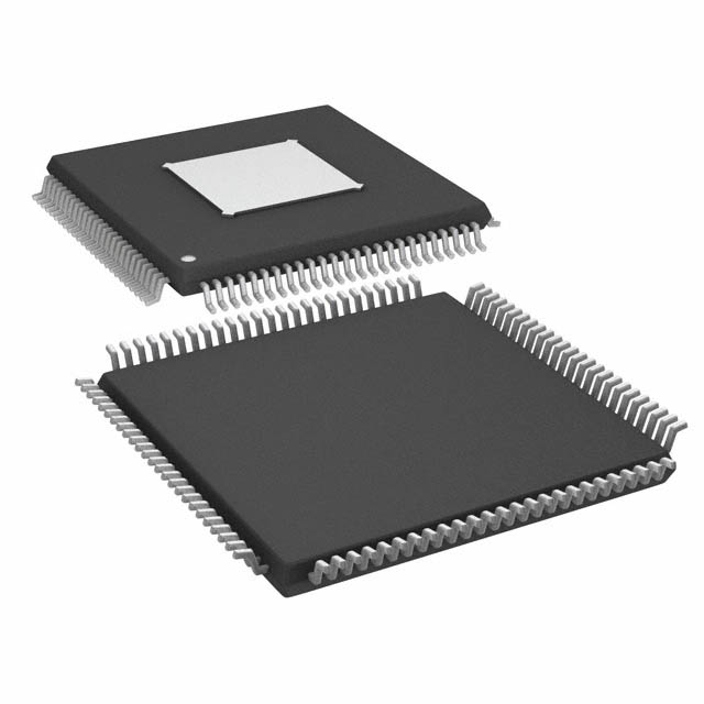
`100-lead, 14 mm * 14 mm, TQFP_EP package
`900 mW per channel with no loadApplication·Automatic test equipment
·Semiconductor test systems
·Board test systems
·Instrumentation and characterization equipmentPinout Specifications
| Parameter |
Rating |
| Supply Voltages |
Positive Supply Voltage (VDD to GND)
|
−0.5 V to +11.0 V |
| Positive VCC Supply Voltage (VCC to GND) |
−0.5 V to +4.0 V |
| Negative Supply Voltage (VSS to GND) |
−6.25 V to +0.5 V |
| Supply Voltage Difference (VDD to VSS) |
−1.0 V to +16.5 V |
| Reference Ground (DUTGND to GND) |
−0.5 V to +0.5 V |
| AGND to DGND |
−0.5 V to +0.5 V |
| VPLUS Supply Voltage (VPLUS to GND) |
−0.5 V to +17.5 V |
| Input Voltages |
Input Common-Mode Voltage |
VSS to VDD |
| Short-Circuit Voltage1 |
−3.0 V to +8.0 V |
| High Speed Input Voltage2 |
0.0 V to VCC |
| High Speed Differential Input Voltage3 |
0.0 V to VCC |
| VREF |
−0.5 V to +5.5 V |
| DUTx I/O Pin Current |
DCL Maximum Short-Circuit Current4 |
±140 mA |
| Temperature |
Operating Temperature, Junction |
125 |
| Storage Temperature Range |
−65 to +150 |
1 RL = 0 , VDUT continuous short-circuit condition, (VH, VL, VT, high-Z, VCOM, clamp modes).
2 DATAxP, DATAxN, RCVxP, RCVxN, under source R = 0 .
3 DATAxP to DATAxN, RCVxP, RCVxN.
4 RL = 0 , VDUTx = 3 V to +8 V; DCL current limit. Continuous short-circuit condition. ADATE305 must current limit and survive continuous short circuit.
Stresses above those listed under Absolute Maximum Ratings may cause permanent damage to the device. This is a stress rating only; functional operation of the device at these or any other conditions above those indicated in the operational section of this specification is not implied. Exposure to absolute maximum rating conditions for extended periods may affect device reliability
DescriptionThe ADATE305 is a complete, single-chip solution that performs the pin electronic functions of the driver, the comparator, and the active load (DCL), per pin PMU, and dc levels for ATE appli-cations. The device also contains an HVOUT driver with a VHH buffer capable of generating up to 13.5 V.
The driver features three active states: data high mode, data low mode, and term mode, as well as an inhibit state. The inhibit state, in conjunction with the integrated dynamic clamp, facili-tates the implementation of a high speed active termination. The ADATE305 supports two output voltage ranges: −2.0 V to +6.0 V and −1.5 V to +6.0 V by adjusting the positive and negative supply voltages.
The ADATE305 can be used as either a dual single-ended drive/ receive channel or a single differential drive/receive channel. Each channel of the ADATE305 features a high speed window comparator per pin for functional testing, as well as a per pin PMU with FV, or FI and MV, or MI functions. All necessary dc levels for DCL functions are generated by on-chip 14-bit DACs. The per pin PMU features an on-chip 16-bit DAC for high accuracy and contains integrated range resistors to minimize external component counts.
The ADATE305 uses a serial bus to program all functional blocks and has an on-board temperature sensor for monitoring the device temperature.

 ADATE305 Data Sheet