Features: . Internal Sample and Hold
. Single +1.9V ±0.1V Operation
. Choice of SDR or DDR output clocking
. Interleave Mode for 2x Sampling Rate
. Multiple ADC Synchronization Capability
. Guaranteed No Missing Codes
. Serial Interface for Extended Control
. Fine Adjustment of Input Full-Scale Range and Off set
. Duty Cycle Corrected Sample ClockApplication. Direct RFD own Conversion
. Digital Oscillo scopes
. Satellite Set-top boxes
. Communications Systems
. Test InstrumentationPinout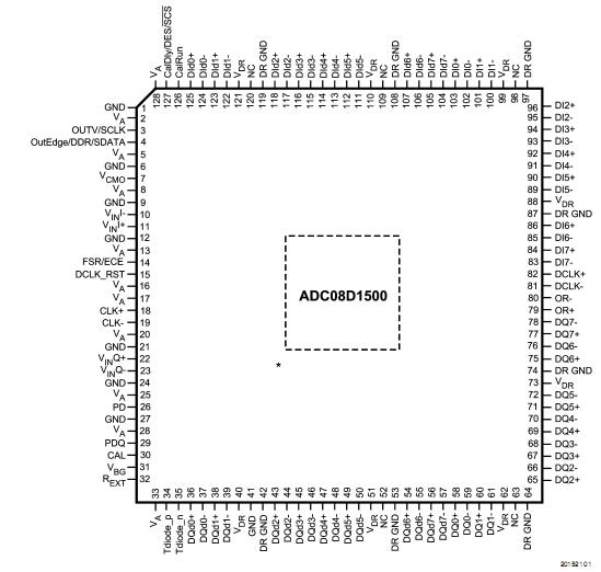 Specifications
| Resolution |
8 bits |
| Channels |
2 Channels |
| SNR |
47 dB |
| SFDR |
56 dB |
| ENOB |
7.4 bits |
| Max Sample Rate |
1500 MSPS |
| Min Sample Rate |
200 MSPS |
| Power Dissipation |
1.8 Watt |
| PowerWise Rating 1 |
3.55 pJ/conv |
| DNL (+/-) |
0.15 LSB |
| INL (+/-) |
0.3 LSB |
| SINAD |
46.3 dB |
| THD dB |
-54.5 dB |
| Min Supply Voltage |
1.8 Volt |
| Max Supply Voltage |
2 Volt |
| Nominal Vin |
0.7 Vpp |
| Temperature Min |
-40 deg C |
| Temperature Max |
85 deg C |
| Data Converter Type |
ADC |
| Automotive Selection Guide |
No |
| PowerWise |
Yes |
| View Using Catalog |
If Military/Aerospace specified devices are required, please contact the National Semiconductor Sales Office/Distributors for availability and specifications.
Supply Voltage (VA,VDR) 2.2V
Voltage on Any Input Pin −0.15Vto(VA+0.15V)
Ground Difference
|GND-DRGND| 0 V to 100 mV
Input Current at AnyPin (Note3) ±25mA
Package Input Current (Note3) ±50mA
Power Dissipation at TA85˚C 2.0W
ESD Susceptibility (Note4)
Human Body Model 2500V
Machine Model 250V
Soldering Temperature, Infrared,
10seconds, (Note5), (Applies
to standard plated pack age only) 235˚C
Storage Temperature −65˚Cto+150˚CDescriptionNote:This product ADC08D1500 is currently indevelopment.-ALL specifications are design targets and are subject to change.
The ADC08D1500 is adual, low power, high performance CMOS analog-to-digital converter that digitizes signals to 8 bits resolution at samplingrate supto 1.7 GSPS.Consuming a typical 1.9 Wattsat 1.5 GSPS from a single1.9 Volt supply, this device is guaranteed to have no missing codes over the full operating temperature range.The unique folding and interpolating architecture, thefully differential comparator design,the innovative design of the internal sample-and-hold amplifier and the self-calibration scheme enablea very flat response of all dynamic para meters beyond Nyquist, producing a high 7.25 ENOB with a 748 MHz input signal and a 1.5 GHz sample rate while providing a 10-18 B.E.R. Output formatting is off setbinary and the LVDS digital out-puts are compliant with IEEE1596.3-1996,with the exception of an adjustable common mode voltagebetween0.8Vand1.2V.
Each converter ADC08D1500 hasa 1:2 demultiplexer that feed stwoLVDS buses and reduces the output datarate on each busto half the sampling rate.Thet wocon verters can be interleaved and used as a single 3GSPS ADC.
The converterADC08D1500 typically consumes less than 3.5m Winthe Power Down Mode and is available in a 128-lead,thermally enhanced exposed padLQFP and operates over the Indus-trial (-40˚CTA+85˚C) temperaturer ange.

 ADC08D1500 Data Sheet