Features: ·Internal Sample-and-Hold
·Single +1.9V ±0.1V Operation
·Choice of SDR or DDR output clocking
·Interleave Mode for 2x Sampling Rate
·Multiple ADC Synchronization Capability
·Guaranteed No Missing Codes
·Serial Interface for Extended Control
·Fine Adjustment of Input Full-Scale Range and Offset
·Duty Cycle Corrected Sample ClockApplication·Direct RF Down Conversion
·Digital Oscilloscopes
·Satellite Set-top boxes
·Communications Systems
·Test InstrumentationPinout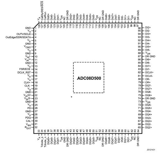 Specifications
| Resolution |
8 bits |
| Channels |
2 Channels |
| SNR |
48 dB |
| SFDR |
55 dB |
| ENOB |
7.5 bits |
| Max Sample Rate |
500 MSPS |
| Min Sample Rate |
200 MSPS |
| Power Dissipation |
1.4 Watt |
| PowerWise Rating 1 |
7.73 pJ/conv |
| DNL (+/-) |
0.15 LSB |
| INL (+/-) |
0.3 LSB |
| SINAD |
47 dB |
| THD dB |
-55 dB |
| Min Supply Voltage |
1.8 Volt |
| Max Supply Voltage |
2 Volt |
| Nominal Vin |
0.7 Vpp |
| Temperature Min |
-40 deg C |
| Temperature Max |
85 deg C |
| Data Converter Type |
ADC |
| Automotive Selection Guide |
Yes |
| PowerWise |
Yes |
| View Using Catalog |
Supply Voltage (VA, VDR) 2.2V
Voltage on Any Input Pin -0.15V to (VA
+0.15V)
Ground Difference
|GND - DR GND|0V to 100 mV
Input Current at Any Pin (Note 3) ±25 mA
Package Input Current (Note 3) ±50 mA
Power Dissipation at TA = 85 2.0 W
ESD Susceptibility (Note 4)
Human Body Model 2500V
Machine Model 250V
Soldering Temperature, Infrared,
10 seconds (Note 5) 235
Storage Temperature -65 to +150
DescriptionThe ADC08D500 is a dual, low power, high performance CMOS analog-to-digital converter that digitizes signals to 8 bits resolution at sampling rates up to 800 MSPS. Consuming a typical 1.4 Watts at 500 MSPS from a single 1.9 Volt supply, this device is guaranteed to have no missing codes over the full operating temperature range. The unique folding and interpolating architecture, the fully differential comparator design, the innovative design of the internal sample-and-hold amplifier and the self-calibration scheme enable a very flat response of all dynamic parameters beyond Nyquist, producing a high 7.5 ENOB with a 250 MHz input signal and a 500 MHz sample rate while providing a 10 -18 B.E.R. Output formatting is offset binary and the LVDS digital outputs are compatible with IEEE 1596.3-1996, with the exception of an adjustable common mode voltage between 0.8V and 1.2V.
Each converter ADC08D500 has a 1:2 demultiplexer that feeds two LVDS buses and reduces the output data rate on each bus to half the sampling rate. The two converters can be interleaved and used as a single 1 GSPS ADC.
The ADC08D500 converter typically consumes less than 3.5 mW in the Power Down Mode and is available in a 128-lead, thermally enhanced exposed pad LQFP and operates over the Industrial (-40°C TA +85°C) temperature range.
Reliability Metrics
| Part Number |
Process |
EFR Reject |
EFR Sample Size |
PPM |
LTA Rejects |
LTA Device Hours |
FITS |
MTTF (Hours) |
| ADC08D500CIYB |
CMOS9 |
1 |
6382 |
157 |
0 |
923000 |
4 |
261903770 |
Note: The Early Failure Rates (EFR) were calculated as point estimate PPM based on rejects and sample size for EFR. The Long Term Failure Rates were calculated at 60% confidence using the Arrhenius equation at 0.7eV activation energy and derating the assumed stress temperature of 150°C to an application temperature of 55°C.For more information on Reliability Metrics, please click here.
Design Tools
| Title |
Size in Kbytes |
Date |
|
|
|
| Evaluation Systems |
17 Kbytes |
29-May-2008 |
View |
|
|
| National GHz ADC Development Platform for Xilinx FPGAs |
6 Kbytes |
5-Feb-2008 |
View |
|
|
If you have trouble printing or viewing PDF file(s), see Printing Problems.
|
The ADC08D500 is a dual, low power, high performance CMOS analog-to-digital converter that digitizes signals to 8 bits resolution at sampling rates up to 800 MSPS. Consuming a typical 1.4 Watts at 500 MSPS from a single 1.9 Volt supply, this device is guaranteed to have no missing codes over the full operating temperature range. The unique folding and interpolating architecture, the fully differential comparator design, the innovative design of the internal sample-andhold amplifier and the self-calibration scheme enable a very flat response of all dynamic parameters beyond Nyquist, producing a high 7.5 ENOB with a 250 MHz input signal and a 500 MHz sample rate while providing a 10-18 B.E.R. Output formatting is offset binary and the LVDS digital outputs are compliant with IEEE 1596.3-1996, with the exception of an adjustable common mode voltage between 0.8V and 1.2V.
Each converter has a 1:2 demultiplexer that feeds two LVDS buses and reduces the output data rate on each bus to half the sampling rate. The two converters can be interleaved and used as a single 1 GSPS ADC.
The converter typically consumes less than 3.5 mW in the Power Down Mode and is available in a 128-lead, thermally enhanced exposed pad LQFP and operates over the Industrial (-40 T
A +85) temperature range.

 ADC08D500 Data Sheet