ADC912A

Features: Low CostLow Transition Noise between Code12-Bit Accurate±1/2 LSB Nonlinearity Error over TemperatureNo Missing Codes at All Temperatures10 s Conversion TimeInternal or External Clock8- or 16-Bit Data Bus CompatibleImproved ESD Resistant DesignLatchup Resistant Epi-CMOS ProcessingLow 95 m...

product image

ADC912A Picture
SeekIC No. : 004274236 Detail

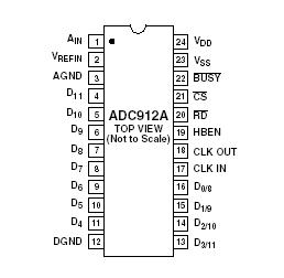
ADC912A: Features: Low CostLow Transition Noise between Code12-Bit Accurate±1/2 LSB Nonlinearity Error over TemperatureNo Missing Codes at All Temperatures10 s Conversion TimeInternal or External Clock8- or ...

floor Price/Ceiling Price

Part Number:
ADC912A
Supply Ability:
5000

Price Break

  • Qty
  • 1~5000
  • Unit Price
  • Negotiable
  • Processing time
  • 15 Days
Total Cost: $ 0.00

SeekIC Buyer Protection PLUS - newly updated for 2013!

  • Escrow Protection.
  • Guaranteed refunds.
  • Secure payments.
  • Learn more >>

Month Sales

268 Transactions

Rating

evaluate  (4.8 stars)

Upload time: 2024/4/28

Payment Methods

All payment methods are secure and covered by SeekIC Buyer Protection PLUS.

Notice: When you place an order, your payment is made to SeekIC and not to your seller. SeekIC only pays the seller after confirming you have received your order. We will also never share your payment details with your seller.
Product Details

Description


Features:

Low Cost
Low Transition Noise between Code
12-Bit Accurate
   ±1/2 LSB Nonlinearity Error over Temperature
   No Missing Codes at All Temperatures
10 s Conversion Time
Internal or External Clock
8- or 16-Bit Data Bus Compatible
Improved ESD Resistant Design
Latchup Resistant Epi-CMOS Processing
Low 95 mW Power Consumption
Space-Saving 24-Lead 0.3" DIP, or 24-Lead SOIC


Application

Data Acquisition Systems
DSP System Front End
Process Control Systems
Portable Instrumentation


Pinout

  Connection Diagram


Specifications

VDD to DGND . . . . . . . . . . . . . . . . . . . . . . . . . 0.3 V to +7 V
VSS to DGND . . . . . . . . . . . . . . . . . . . . . . . . . +0.3 V to 7 V
VREFIN to DGND . . . . . . . . . . . . . . . . . . . . . . . . . . VSS to VDD
AGND to DGND . . . . . . . . . . . . . . . .  .  0.3 V to VDD + 0.3 V
AIN to AGND . . . . . . . . . . . . . . . . . . . . . . . .  .15 V to +15 V
Digital Input Voltage to DGND,
Pins 17, 1921 . . . . . . . . . . . . . . . . . 0.3 V to VDD + 0.3 V
Digital Output Voltage to DGND,
Pins 411, 1316, 18, 22 . . . . . . . .  0.3 V to VDD + 0.3 V
Operating Temperature Range
Extended Industrial: ADC912A/F . . . . . . .40°C to +85°C
Storage Temperature . . . . . . . . . . . . . . 65°C to +150°C
Lead Temperature (Soldering, 10 sec) . . . . . . . . . . . 300°C
Maximum Junction Temperature (TJ max) . . . . . . . . . 150°C
Package Power Dissipation . . . . . . . . . . . . (TJ maxTA)/JA
Thermal Resistance JA
Plastic DIP . . . . . . . . . . . . . . . . . . . . . . . . . . . . . . . 57°C/W
SOIC-24 . . . . . . . . . . . . . . . . . . . . . . . . . . . . . . . . . . .70°C


Description

The ADC912A is a monolithic 12-bit accurate CMOS A/D converter. It contains a complete successive-approximation A/D converter built with a high-accuracy D/A converter, a precision bipolar transistor high-speed comparator, and successiveapproximation logic including three-state bus interface for logic compatibility. The accuracy of the ADC912A results from the addition of precision bipolar transistors to Analog Devices' advanced-oxide isolated silicon-gate CMOS process. Particular attention was paid to the reduction of transition noise between adjacent codes achieving a 1/6 LSB uncertainty. The low noise design produces the same digital output for dc analog inputs not located at a transition voltage, see Figures 1 and 2. NPN digital output transistors provide excellent bus interface timing, 125 ns access and bus disconnect time which results in faster data transfer without the need for wait states. An external 1.25 MHz clock provides a 10 µs conversion time.

In stand-alone applications an internal clock can be used with external crystal.

An external negative five-volt reference sets the 0 V to 10 V input range. Plus 5 V and minus 12 V power supplies result in 95 mW of total power consumption.


Customers Who Bought This Item Also Bought

Margin,quality,low-cost products with low minimum orders. Secure your online payments with SeekIC Buyer Protection.
Static Control, ESD, Clean Room Products
Test Equipment
Potentiometers, Variable Resistors
Power Supplies - External/Internal (Off-Board)
Optical Inspection Equipment
Fans, Thermal Management
View more