ADCMP572

Features: *3.3 V/5.2 V single-supply operation *150 ps propagation delay *15 ps overdrive and slew rate dispersion *8 GHz equivalent input risetime bandwidth *80 ps minimum pulse width *35 ps typical output rise/fall *10 ps deterministic jitter (DJ) *200 fs random jitter (RJ) *On-chip terminations...

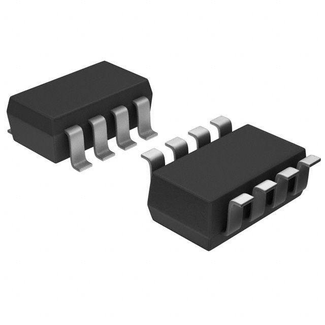
product image

ADCMP572 Picture
SeekIC No. : 004274275 Detail

ADCMP572: Features: *3.3 V/5.2 V single-supply operation *150 ps propagation delay *15 ps overdrive and slew rate dispersion *8 GHz equivalent input risetime bandwidth *80 ps minimum pulse width *35 ps typica...

floor Price/Ceiling Price

Part Number:
ADCMP572
Supply Ability:
5000

Price Break

  • Qty
  • 1~5000
  • Unit Price
  • Negotiable
  • Processing time
  • 15 Days
Total Cost: $ 0.00

SeekIC Buyer Protection PLUS - newly updated for 2013!

  • Escrow Protection.
  • Guaranteed refunds.
  • Secure payments.
  • Learn more >>

Month Sales

268 Transactions

Rating

evaluate  (4.8 stars)

Upload time: 2025/12/12

Payment Methods

All payment methods are secure and covered by SeekIC Buyer Protection PLUS.

Notice: When you place an order, your payment is made to SeekIC and not to your seller. SeekIC only pays the seller after confirming you have received your order. We will also never share your payment details with your seller.
Product Details

Description


Features:

*3.3 V/5.2 V single-supply operation
*150 ps propagation delay
*15 ps overdrive and slew rate dispersion
*8 GHz equivalent input risetime bandwidth
*80 ps minimum pulse width
*35 ps typical output rise/fall
*10 ps deterministic jitter (DJ)
*200 fs random jitter (RJ)
*On-chip terminations at both input pins
*Robust inputs with no output phase reversal
*Resistor programmable hysteresis
*Differential latch control
*Power supply rejection > 70 dB


Application

Automatic test equipment (ATE)
High speed instrumentation
Pulse spectroscopy
Medical imaging and diagnostics
High speed line receivers
Threshold detection
Peak and zero-crossing detectors
High speed trigger circuitry
Clock and data signal restoration


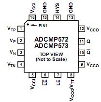
Pinout

  Connection Diagram


Specifications

Parameter Rating
SUPPLY VOLTAGES
Input Supply Voltage (VCCI to GND)
Output Supply Voltage
(VCCO to GND)
Positive Supply Differential
(VCCI − VCCO )

−0.5 V to +6.0 V
−0.5 V to +6.0 V

−0.5 V to +3.5 V

INPUT VOLTAGES
Input Voltage
Differential Input Voltage
Input Voltage, Latch Enable
−0.5 V to VCCI + 0.5 V
±(VCCI + 0.5 V)
−0.5 V to V + 0.5 V
HYSTERESIS CONTROL PIN
Applied Voltage (HYS to GND)
Maximum Input/Output Current
−0.5 V to +1.5 V
±1 mA
OUTPUT CURRENT
ADCMP572 (CML)
ADCMP573 (RSPECL)
±20 mA
−35 mA
TEMPERATURE
Operating Temperature, Ambient
Operating Temperature, Junction
Storage Temperature Range
−40°C to +85°C
125°C
−65°C to +150°C


Logic Output CML
# Per Pkg 1
Prop Delay (ns)typ 0.15ns
Voltage Supply (V) 3.3 to 5
Supply Current 44mA
Min Pulse Width 80ps
Package 16-Lead LFCSP
Output Rise/Fall Time 35 ps
Latch Enable Pin X
Jitter <200 fs


Description

The ADCMP572/ADCMP573 are ultrafast comparators fabricated on Analog Devices, Inc. ' s proprietary XFCB3 SiliconGermanium (SiGe) bipolar process. The ADCMP572 featuresCML output drivers, and the ADCMP573 features reduced swing PECL (RSPECL) output drivers.

Both devices ADCMP572/ADCMP573 offer 150 ps propagation delay and 100 ps minimum pulse width for 10 Gbps operation with 200 fs RMS random jitter (RJ). Overdrive and slew rate dispersion is typically less than 15 ps.

A flexible power supply scheme allows either device to operate with a single +3.3 V positive supply and a −0.2 V to +1.2 V input signal range, or with split input/output supplies to support a wider −0.2 V to +3.2 V input signal range and an independent range of output levels. 50 Ω on-chip termination resistors are provided at both inputs with the optional capability to leave open (on an individual pin basis) for applications requiring high impedance inputs.

The CML output stage of ADCMP572/ADCMP573 is designed to directly drive 400 mV into 50 Ω transmission lines terminated to between 3.3 V to 5.2 V. The RSPECL output stage is designed to drive 400 mV into 50 Ω terminated to VCCO − 2 V and is compatible with several commonly used PECL logic families. The comparator input stage offers robust protection against large input overdrive, and the outputs do not phase reverse when the valid input signal range is exceeded. High speed latch and programmable hysteresis features are also provided.

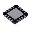
The ADCMP572/ADCMP573 are available in a 16-lead LFCSP package.


Customers Who Bought This Item Also Bought

Margin,quality,low-cost products with low minimum orders. Secure your online payments with SeekIC Buyer Protection.
Audio Products
Tapes, Adhesives
803
Computers, Office - Components, Accessories
Soldering, Desoldering, Rework Products
Fans, Thermal Management
Discrete Semiconductor Products
View more