Features: 180 ps propagation delay 25 ps overdrive and slew rate dispersion 8 GHz equivalent input rise time bandwidth 100 ps minimum pulse width 37 ps typical output rise/fall 10 ps deterministic jitter (DJ) 200 fs random jitter (RJ) −2 V to +3 V input range with +5 V/−5 V supplies O...
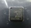
ADCMP580: Features: 180 ps propagation delay 25 ps overdrive and slew rate dispersion 8 GHz equivalent input rise time bandwidth 100 ps minimum pulse width 37 ps typical output rise/fall 10 ps deterministic ...
SeekIC Buyer Protection PLUS - newly updated for 2013!
268 Transactions
All payment methods are secure and covered by SeekIC Buyer Protection PLUS.
Parameter | Rating |
SUPPLY VOLTAGES Positive Supply Voltage (VCCI to GND) Negative Supply Voltage (VEE to GND) Logic Supply Voltage (VCCO to GND) |
−0.5 V to +6.0 V 6.0 V to +0.5 V −0.5 V to +6.0 V |
INPUT VOLTAGES Input Voltage Differential Input Voltage Input Voltage, Latch Enable |
−3.0 V to +4.0 V −2 V to +2 V −2.5 V to +5.5 V |
HYSTERESIS CONTROL PIN Applied Voltage (HYS to VEE) Maximum Input/Output Current |
−5.5 V to +0.5 V 1 mA |
OUTPUT CURRENT ADCMP580 (CML) ADCMP581 (NECL) ADCMP582 (PECL) |
−25 mA −40 mA −40 mA |
TEMPERATURE Operating Temperature, Ambient Operating Temperature, Junction Storage Temperature Range |
−40°C to +125°C 125°C −65°C to +150°C |
The ADCMP580/ADCMP581/ADCMP582 are ultrafast voltage comparators fabricated on Analog Devices' proprietary XFCB3 Silicon Germanium (SiGe) bipolar process. The ADCMP580 features CML output drivers; the ADCMP581 features reduced swing ECL (negative ECL) output drivers; and the ADCMP582 features reduced swing PECL (positive ECL) output drivers.
All three comparators ADCMP580/ADCMP581/ADCMP582 offer 180 ps propagation delay and 100 ps minimum pulse width for 10 Gbps operation with 200 fs random jitter (RJ). Overdrive and slew rate dispersion are typically less than 15 ps.
The ADCMP580/ADCMP581/ADCMP582's ±5 V power supplies enable a wide −2 V to +3 V input range with logic levels referenced to the CML/NECL/PECL outputs. The inputs have 50 on-chip termination resistors with the optional capability to be left open (on an individual pin basis) for applications requiring high impedance input.
The CML output stage of ADCMP580/ADCMP581/ADCMP582 is designed to directly drive 400 mV into 50 transmission lines terminated to ground. The NECL output stages are designed to directly drive 400 mV into 50 terminated to −2 V. The PECL output stages are designed to directly drive 400 mV into 50 terminated to VCCO − 2 V. High speed latch and programmable hysteresis are also provided. The differential latch input controls are also 50 terminated to an independent VTT pin to interface to either CML or ECL or to PECL logic.
The ADCMP580/ADCMP581/ADCMP582 are available in a 16-lead LFCSP package.