
ADG1209: Features:
 ADG1209 Data Sheet
floor Price/Ceiling Price
- Part Number:
- ADG1209
- Supply Ability:
- 5000
Price Break
- Qty
- 1~5000
- Unit Price
- Negotiable
- Processing time
- 15 Days
SeekIC Buyer Protection PLUS - newly updated for 2013!
- Escrow Protection.
- Guaranteed refunds.
- Secure payments.
- Learn more >>
Month Sales
268 Transactions
Payment Methods
All payment methods are secure and covered by SeekIC Buyer Protection PLUS.
-
Recent History
- What is this?


Description
Features:
Specifications
|
Parameter |
Rating |
|
VDD to VSS |
35 V |
|
VDD to GND |
−0.3 V to +25 V |
|
VSS to GND |
+0.3 V to −25 V |
|
Analog, Digital Inputs1 |
VSS − 0.3 V to VDD + 0.3 V or30 mA (whichever occurs first) |
|
Continuous Current, S or D |
30 mA |
|
Peak Current, S or D (Pulsed at 1 ms, 10% Duty Cycle max) |
100 mA |
|
Operating Temperature Range |
|
|
Industrial (Y Version) |
40°C to +125°C |
|
Storage Temperature |
65°C to +150°C |
|
Junction Temperature |
150°C |
|
TSSOP, JA, Thermal Impedance |
112°C/W |
|
LFCSP_VQ, JA, Thermal Impedance |
30.4°C/W |
|
Reflow Soldering Peak |
260(+0/−5)°C |
|
Temperature (Pb-Free) |
Description
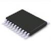
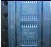
The ADG1208 and ADG1209 are monolithic, iCMOS analog multiplexers comprising eight single channels and four differential channels, respectively. The ADG1208 and ADG1209 switches one of eight inputs to a common output as determined by the 3-bit binary address lines A0, A1, and A2. The ADG1208 and ADG1209 switches one of four differential inputs to a common differential output as determined by the 2-bit binary address lines A0 and A1. An EN input on both devices is used to enable or disable the device. When disabled, all channels are switched off. When on, each channel conducts equally well in both directions and has an input signal range that extends to the supplies.
The iCMOS (industrial CMOS) modular manufacturing process combines high voltage CMOS (complementary metal-oxide semiconductor) and bipolar technologies. ADG1208 and ADG1209 enable the development of a wide range of high performance analog ICs capable of 33 V operation in a footprint that no other generation of high voltage parts has been able to achieve. Unlike analog ICs using conventional CMOS processes, iCMOS components can tolerate high supply voltages while providing increased performance, dramatically lower power consumption, and reduced package size.
The ultralow capacitance and exceptionally low charge injection of these multiplexers make ADG1208 and ADG1209 be ideal solutions for data acquisition and sample-and-hold applications, where low glitch and fast settling are required. Figure 2 shows that there is minimum charge injection over the entire signal range of the device. iCMOS construction also ensures ultralow power dissipation, making the parts ideally suited for portable and battery powered instruments.
Customers Who Bought This Item Also Bought
-
 US $$0.50 - 1.00 / PieceSupply Ability:10000Week
 -
 US $$0.30 - 0.50 / PieceSupply Ability:100000Day
 -
 US $$3.40 - 5.60 / PieceSupply Ability:1Day
 -
 US $$4.00 - 4.20 / PieceSupply Ability:10000Week
 -
 US $$3.00 - 3.00 / PieceSupply Ability:1000Day

Consumer Protection
Escrow service
What is Seekic Buyer Protection?
Faithfully describe
24 hours delivery
7 days Changing or Refunding
New Buyer Guide
New hand registration
How to buy
Get to know Seekic.com
About member Club

Freight and Payment
Recommended logistics
Recommended bank
Transaction security
Complaint and Report
Security Code
SeekIC bank information
Blacklist
© 2008-2012 SeekIC.com Corp.All Rights Reserved.