ADG406

Features: 44 V Supply Maximum RatingsVSS to VDD Analog Signal RangeLow On Resistance (80 Ω max)Low PowerFast SwitchingtON < 160 nstOFF < 150 nsBreak Before Make Switching ActionPlug-In Upgrade for DG506A/ADG506A, DG507A/ADG507A, DG526/ADG526AADG406/ADG407 are Plug-In Replacements for D...

product image

ADG406 Picture
SeekIC No. : 004274912 Detail

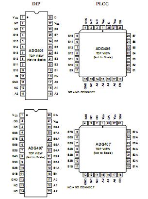
ADG406: Features: 44 V Supply Maximum RatingsVSS to VDD Analog Signal RangeLow On Resistance (80 Ω max)Low PowerFast SwitchingtON < 160 nstOFF < 150 nsBreak Before Make Switching ActionPlug-In U...
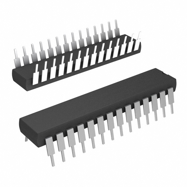
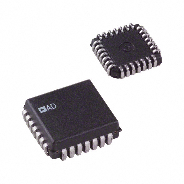
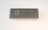
floor Price/Ceiling Price

Part Number:
ADG406
Supply Ability:
5000

Price Break

  • Qty
  • 1~5000
  • Unit Price
  • Negotiable
  • Processing time
  • 15 Days
Total Cost: $ 0.00

SeekIC Buyer Protection PLUS - newly updated for 2013!

  • Escrow Protection.
  • Guaranteed refunds.
  • Secure payments.
  • Learn more >>

Month Sales

268 Transactions

Rating

evaluate  (4.8 stars)

Upload time: 2024/4/26

Payment Methods

All payment methods are secure and covered by SeekIC Buyer Protection PLUS.

Notice: When you place an order, your payment is made to SeekIC and not to your seller. SeekIC only pays the seller after confirming you have received your order. We will also never share your payment details with your seller.
Product Details

Description


Features:

44 V Supply Maximum Ratings
VSS to VDD Analog Signal Range
Low On Resistance (80 Ω max)
Low Power
Fast Switching
tON < 160 ns
tOFF < 150 ns
Break Before Make Switching Action
Plug-In Upgrade for DG506A/ADG506A, DG507A/ADG507A, DG526/ADG526A
ADG406/ADG407 are Plug-In Replacements for DG406/DG407


Application

Audio and Video Routing
Automatic Test Equipment
Data Acquisition Systems
Battery Powered Systems
Sample Hold Systems
Communication Systems
Avionics


Pinout

  Connection Diagram

ADG406 Diagram


Specifications

VDD to VSS . . . . . . . . . . . . . . . . . . . . . . . . . . . . . . . . . . +44 V
VDD to GND . . . . . . . . . . . . . . . . . . . . . . . . . . 0.3 V to +25 V
VSS to GND . . . . . . . . . . . . . . . . . . . . . . . . . . +0.3 V to 25 V
Analog, Digital Inputs2. . . . . . . . . . . VSS 2 V to VDD + 2 V
or 20 mA, Whichever Occurs First
Continuous Current, S or D . . . . . . . . . . . . . . . . . . . . .20 mA
Peak Current, S or D . . . . . . . . . . . . . . . . . . . . . . . . . . 40 mA
(Pulsed at 1 ms, 10% Duty Cycle Max)
Operating Temperature Range
Industrial (B Version) . . . . . . . . . . . . . . . . .40°C to +85°C
Extended (T Version) . . . . . . . . . . . . . . . . 55°C to +125°C
Storage Temperature Range . . . . . . . . . 65°C to +150°C
Junction Temperature . . . . . . . . . . . . . . . . . . . . . . +150°C
Plastic Package
JA, Thermal Impedance . . . . . . . . . . . . . . . . . . . . 75°C/W
Lead Temperature, Soldering (10 sec) . . . . . . . . . .+260°C
PLCC Package
JA, Thermal Impedance . . . . . . . . . . . . . . . . . . . 80°C/W
Lead Temperature, Soldering
Vapor Phase (60 sec) . . . . . . . . . . . . . . . . . . . . . +215°C
Infrared (15 sec) . . . . . . . . . . . . . . . . . . . . . . . . . . +220°C
SSOP Package
JA, Thermal Impedance . . . . . . . . . . . . . . . . . . 122°C/W
Lead Temperature, Soldering
Vapor Phase (60 sec) . . . . . . . . . . . . . . . . . . . . . +215°C
Infrared (15 sec) . . . . . . . . . . . . . . . . . . . . . . . . . +220°C


Sw/Mx Function x # (16:1) x 1
Interface Type Parallel
Available Packages DIP,LCC
Max Analog Signal Range Vss to Vdd
Ron (Ohms) 50Ohms
Ron Match (Ohms) 4Ohms
Cs (OFF) 5pF
Cs, Cd (ON) 60pF
Off Isolation (-dB) 75dB
Bandwidth n/a


Description

The ADG406/ADG407/ADG426 are monolithic CMOS analog multiplexers. TheADG406/ADG407/ADG426 switch one of sixteen inputs to a common output as determined by the 4-bit binary address lines A0, A1, A2 and A3. The ADG426 has on-chip address and control latches that facilitate microprocessor interfacing. The ADG406/ADG407/ADG426 switch one of eight differential inputs to a common differential output as determined by the 3-bit binary address lines A0, A1 and A2. An EN input on all devices is used to enable or disable the device. When disabled, all channels are switched OFF.

The ADG406/ADG407/ADG426 are designed on an enhanced LC2 MOS process that provides low power dissipation yet gives high switching speed and low on resistance. These features make the parts suitable for high speed data acquisition systems and audio signal switching. Low power dissipation makes the parts suitable for battery powered systems. Each channel conducts equally well in both directions when ON and has an input signal range which extends to the supplies. In the OFF condition, signal levels up to the supplies are blocked. All channels exhibit break before make switching action preventing momentary shorting when switching channels. Inherent in the design is low charge injection for minimum transients when switching the digital inputs.


Customers Who Bought This Item Also Bought

Margin,quality,low-cost products with low minimum orders. Secure your online payments with SeekIC Buyer Protection.
Connectors, Interconnects
Sensors, Transducers
Potentiometers, Variable Resistors
LED Products
Cables, Wires - Management
Circuit Protection
View more