ADG528F

Features: Low On Resistance (300 Typ)Fast Switching TimestON 250 ns MaxtOFF 250 ns MaxLow Power Dissipation (3.3 mW Max)Fault and Overvoltage Protection (40 V to +55 V)All Switches OFF with Power Supply OFFAnalog Output of ON Channel Clamped within PowerSupplies if an Overvoltage OccursLatch-Up Pr...

product image

ADG528F Picture
SeekIC No. : 004275046 Detail

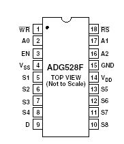
ADG528F: Features: Low On Resistance (300 Typ)Fast Switching TimestON 250 ns MaxtOFF 250 ns MaxLow Power Dissipation (3.3 mW Max)Fault and Overvoltage Protection (40 V to +55 V)All Switches OFF with Power Su...
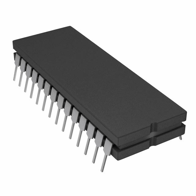
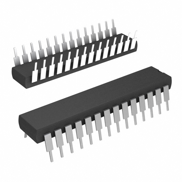
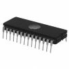
floor Price/Ceiling Price
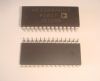
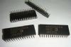
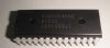
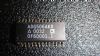
Part Number:
ADG528F
Supply Ability:
5000

Price Break

  • Qty
  • 1~5000
  • Unit Price
  • Negotiable
  • Processing time
  • 15 Days
Total Cost: $ 0.00

SeekIC Buyer Protection PLUS - newly updated for 2013!

  • Escrow Protection.
  • Guaranteed refunds.
  • Secure payments.
  • Learn more >>

Month Sales

268 Transactions

Rating

evaluate  (4.8 stars)

Upload time: 2024/4/29

Payment Methods

All payment methods are secure and covered by SeekIC Buyer Protection PLUS.

Notice: When you place an order, your payment is made to SeekIC and not to your seller. SeekIC only pays the seller after confirming you have received your order. We will also never share your payment details with your seller.
Product Details

Description


Features:

Low On Resistance (300 Typ)
Fast Switching Times
   tON 250 ns Max
   tOFF 250 ns Max
Low Power Dissipation (3.3 mW Max)
Fault and Overvoltage Protection (40 V to +55 V)
All Switches OFF with Power Supply OFF
Analog Output of ON Channel Clamped within Power
Supplies if an Overvoltage Occurs
Latch-Up Proof Construction
Break before Make Construction
TTL and CMOS Compatible Inputs


Application

Existing Multiplexer Applications (Both Fault-Protected and Nonfault-Protected)
New Designs Requiring Multiplexer Functions


Pinout

  Connection Diagram


Specifications

VDD to VSS . . . . . . . . . . . . . . . . . . . . . . . . . . . . . . . . . . . 44 V
VDD to GND . . . . . . . . . . . . . . . . . . . . . . . . . .0.3 V to +25 V
VSS to GND . . . . . . . . . . . . . . . . . . . . . . . . . .+0.3 V to 25 V
VEN, VA Digital Input . . . . . . . 0.3 V to VDD + 2 V or 20 mA,
Whichever Occurs First
VS, Analog Input Overvoltage with Power ON . . . VSS 25 V
to VDD + 40 V
VS, Analog Input Overvoltage with Power OFF
. . . . . . . . . . . . . . . . . . . . . . . . . . . . . . . . . . . .40 V to +55 V
Continuous Current, S or D . . . . . . . . . . . . . . . . . . . . . 20 mA
Peak Current, S or D
(Pulsed at 1 ms, 10% Duty Cycle max) . . . . . . . . . . . . 40 mA
Operating Temperature Range
Industrial (B Version) . . . . . . . . . . . . . . . .40°C to +85°C
Storage Temperature Range . . . . . . . . . 65°C to +150°C
Junction Temperature . . . . . . . . . . . . . . . . . . . . . . . . 150°C
Plastic Package
JA, Thermal Impedance
16-Lead . . . . . . . . . . . . . . . . . . . . . . . . . . . . . . . . . .. 117°C
18-Lead . . . . . . . . . . . . . . . . . . . . . . . . . . . . . . . .. . . 110°C
Lead Temperature, Soldering (10 sec) . . . . . . . . . . ..260°C
SOIC Package
JA, Thermal Impedance
Narrow Body . . . . . . . . . . . . . . . . . . . . . . . . . . . . ...77°C/W
Wide Body . . . . . . . . . . . . . . . . . . . . . . . . . . . . . ... 75°C/W
Lead Temperature, Soldering
Vapor Phase (60 sec) . . . . . . . . . . . . . . . . . . . . . . .. 215°C
Infrared (15 sec) . . . . . . . . . . . . . . . . . . . . . . . . . .. .220°C
PLCC Package
JA, Thermal Impedance . . . . . . . . . . . . . . . . . . . . 90°C/W
Lead Temperature, Soldering
Vapor Phase (60 sec) . . . . . . . . . . . . . . . . . . . . . . . .215°C
Infrared (15 sec) . . . . . . . . . . . . . . . . . . . . . . . . . . . 220°C


Description

The ADG508F, ADG509F, and ADG528F are CMOS analog multiplexers, the ADG508F and ADG528F comprising eight single channels and the ADG509F comprising four differential channels. These multiplexers provide fault protection. Using a series n-channel, p-channel, n-channel MOSFET structure, both device and signal source protection is provided in the event of an overvoltage or power loss. The multiplexer can withstand continuous overvoltage inputs from 40 V to +55 V. During fault conditions, the multiplexer input (or output) appears as an open circuit and only a few nanoamperes of leakage current will flow. This protects not only the multiplexer and the circuitry driven by the multiplexer, but also protects the sensors or signal sources that drive the multiplexer.

The ADG508F and ADG528F switch one of eight inputs to a common output as determined by the 3-bit binary address lines A0, A1, and A2. The ADG509F switches one of four differential inputs to a common differential output as determined by the 2-bit binary address lines A0 and A1. The ADG528F has on-chip address and control latches that facilitate microprocessor interfacing. An EN input on each device is used to enable or disable the device. When disabled, all channels are switched OFF.


Customers Who Bought This Item Also Bought

Margin,quality,low-cost products with low minimum orders. Secure your online payments with SeekIC Buyer Protection.
RF and RFID
Crystals and Oscillators
Batteries, Chargers, Holders
Resistors
Hardware, Fasteners, Accessories
Programmers, Development Systems
View more