Features: `+1.8 V to +5.5 V Single Supply
`4 (Max) On Resistance
`0.75 (Typ) On-Resistance Flatness
`3 dB Bandwidth >200 MHz
`Rail-to-Rail Operation
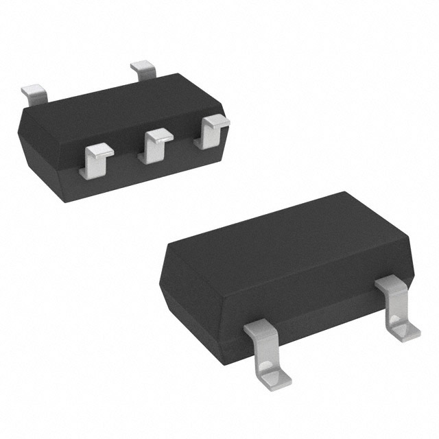
`6-Lead SOT-23 Package, 8-Lead mSOIC Package
`Fast Switching Times
tON 20 ns
tOFF 6 ns
`Typical Power Consumption (<0.01 mW)
`TTL/CMOS CompatibleApplication·Battery Powered Systems
·Communication Systems
·Sample Hold Systems
·Audio Signal Routing
·Video Switching
·Mechanical Reed Relay ReplacementPinout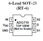 Specifications
VDD to GND . . . . . . . . . . . . . . . . . . . . .. 0.3 V to +7 V
Analog, Digital Inputs2 . . . . . 0.3 V to VDD + 0.3 V or
30 mA, Whichever Occurs First
Peak Current, S or D . . . . . . . . . . . . . . . . . . . . .100 mA
(Pulsed at 1 ms, 10% Duty Cycle max)
Continuous Current, S or D . . . . . . . . . . . . . . . . .30 mA
Operating Temperature Range
Industrial (B Version) . . . . . . . . 40°C to +85°C
Storage Temperature Range . . . . . 65°C to +150°C
Junction Temperature . . . . . . . . . . . . . . . . . . . +150°C
mSOIC Package, Power Dissipation . . . . . . . . .315 mW
qJA Thermal Impedance . . . . . . . . . . . . . . 206°C/W
qJC Thermal Impedance . . . . . . . . . . . . . . 44°C/W
SOT-23 Package, Power Dissipation . . . . . . . 282 mW
qJA Thermal Impedance . . . . . . . . . . . . .229.6°C/W
qJC Thermal Impedance . . . . . . . . . . . . .91.99°C/W
Lead Temperature, Soldering
Vapor Phase (60 sec) . . . . . . . . . . . . . . . . . . . . . . . . +215°C
Infrared (15 sec) . . . . . . . . . . . . . . . . . . . . . . . . . . . . +220°C
ESD . . . . . . . . . . . . . . . . . . . . . . . . . . . . . . . . . . . . . . . . . . 1 kV
NOTES
1 Stresses above those listed under Absolute Maximum Ratings may cause permanent damage to the device. This is a stress rating only; functional operation of the device at these or any other conditions above those listed in the operational sections of this specification is not implied. Exposure to absolute maximum rating conditions for extended periods may affect device reliability. Only one absolute maximum rating may be applied at any one time.
2 Overvoltages at IN, S or D will be clamped by internal diodes. Current should be limited to the maximum ratings given.
DescriptionThe ADG719 is a monolithic CMOS SPDT switch. This switch is designed on a submicron process that provides low power dissipation yet gives high switching speed, low on resistance and low leakage currents.
The ADG719 can operate from a single supply range of +1.8 V to +5.5 V, making it ideal for use in battery-powered instruments and with the new generation of DACs and ADCs from Analog Devices.
Each switch of the ADG719 conducts equally well in both directions when on. The ADG719 exhibits break-before-make switching action. Because of the advanced submicron process, 3 dB bandwidths of greater than 200 MHz can be achieved. The ADG719 is available in a 6-lead SOT-23 package and an 8-lead mSOIC package.

 ADG719 Data Sheet