Features: `1.8 V to 5.5 V Single Supply
`±2.5 V Dual Supply Operation
`3.5 On Resistance
`0.5 On Resistance Flatness
`Rail to Rail Operation
`30ns Switching Times
`Single 32 to 1 Channel Multiplexer
`Dual/Differential 16 to 1 Channel Multiplexer
`TTL/CMOS Compatible Inputs
`For Functionally Equivalent devices with Serial Interface
See ADG725/ADG731Application·Optical Applications
·Data Acquisition Systems
·Communication Systems
·Relay replacement
·Audio and Video Switching
·Battery Powered Systems
·Medical Instrumentation
·Automatic Test EquipmentPinout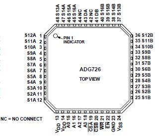
 Specifications
VDD to VSS ........................................................................+7 V
VDD to GND .......................................................0.3 V to +7 V
VSS to GND ..........................................................+0.3 V to -7 V
Analog Inputs2.............................. VSS - 0.3 V to VDD +0.3 Vor
30 mA, Whichever Occurs First
Digital Inputs2 .......................................-0.3V to VDD +0.3 V or
30 mA, Whichever Occurs First
Peak Current, S or D 60mA
(Pulsed at 1 ms, 10% Duty Cycle max)
Continuous Current, S or D ..............................................30mA
Operating Temperature Range
Industrial (B Version) ...................................40°C to +85°C
Storage Temperature Range .....................65°C to +150°C
Junction Temperature .................................................+150°C
48 lead CSP JA Thermal Impedance ........................TBD°C/W
48 lead TQFP JA Thermal Impedance ......................TBD°C/W
Lead Temperature, Soldering (10seconds) ...................300°C
IR Reflow, Peak Temperature .....................................+220°C
NOTES
1 Stresses above those listed under "Absolute Maximum Ratings" may cause permanent damage to the device. This is a stress rating only and functional operation of the device at these or any other conditions above those listed in the operational sections of this specification is not implied. Exposure to absolute maximum rating conditions for extended periods may affect device reliability. Only one absolute maximum rating may be applied at any one time.
2 Overvoltages at A, WR, RS, S or D will be clamped by internal diodes. Current should be limited to the maximum ratings given.
| Sw/Mx Function x # |
(16:1) x 2 |
| Interface Type |
Parallel |
| Available Packages |
CSP,QFP |
| Max Analog Signal Range |
Vss to Vdd |
| Ron (Ohms) |
4Ohms |
| Ron Match (Ohms) |
0.3Ohms |
| Cs (OFF) |
13pF |
| Cs, Cd (ON) |
175pF |
| Off Isolation (-dB) |
72dB |
| Bandwidth |
34MHz |
DescriptionThe ADG726/ADG732 are monolithic CMOS 32 channel/dual 16 channel analog multiplexers. The ADG726/ADG732 switches one of thirty-two inputs (S1-S32) to a common output, D, as determined by the 5-bit binary address lines A0, A1, A2, A3 and A4. The ADG726/ADG732 switches one of sixteen inputs as determined by the four bit binary address lines, A0, A1, A2 and A3.
On chip latches facilitate microprocessor interfacing. The ADG726/ADG732 may also be configured for differential operation by tying CSA and CSB together. AnEN input is used to enable or disable the devices. When disabled, all channels are switched OFF.
These multiplexers are designed on an enhanced submicron process that provides low power dissipation yet gives high switching speed, very low on resistance and leakage currents. ADG726/ADG732 operates from single supply of 1.8V to 5.5V and ±2.5 V dual supply, making them ideally suited to a variety of applications. On resistance is in the region of a few Ohms and is closely matched between switches and very flat over the full signal range. These parts can operate equally well as either Multiplexers or De-Multiplexers and have an input signal range which extends to the supplies.In the OFF condition, signal levels up to the supplies are blocked. All channels exhibit break before make switching action preventing momentary shorting when switching channels.
ADG726/ADG732 are available in either 48 lead LFCSP or TQFP package.

 ADG726 Data Sheet