Features: Voltage-controlled amplifier/attenuator Operating frequency 10 MHz to 3 GHz Optimized for controlling output power High linearity: OIP3 31 dBm @ 900 MHz Output noise floor: −150 dBm/Hz @ 900 MHz 50 input and output impedances Single-ended or differential operation Wide gain-contr...
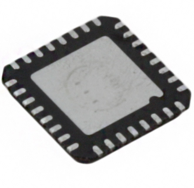
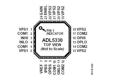
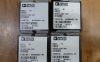
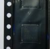
ADL5330: Features: Voltage-controlled amplifier/attenuator Operating frequency 10 MHz to 3 GHz Optimized for controlling output power High linearity: OIP3 31 dBm @ 900 MHz Output noise floor: −150 dBm...
SeekIC Buyer Protection PLUS - newly updated for 2013!
268 Transactions
All payment methods are secure and covered by SeekIC Buyer Protection PLUS.


| Parameter | Rating |
| Supply Voltage VPS1, VPS2 RF Input Power at Maximum Gain OPHI, OPLO ENBL GAIN Internal Power Dissipation JA (with Pad Soldered to Board) Maximum Junction Temperature Operating Temperature Range Storage Temperature Range Lead Temperature Range (Soldering 60 sec) |
5.5 V 5 dBm at 50 5.5 V VPS1, VPS2 2.5 V 1.1 W 60°C/W 150°C −40°C to +85°C −65°C to +150°C 300°C |
| Gain Control | Analog |
| -3 dB BW (MHz) | 3000MHz |
| Gain Low End (dB) | -34dB |
| Gain High End (dB) | +22dB |
| Number of Channels | 1 |
| Supply Voltage (V) | +5V |
| Supply Current | 240mA |
The ADL5330 is a high performance, voltage-controlled variable gain amplifier/attenuator for use in applications with frequencies up to 3 GHz. The balanced structure of the signal path minimizes distortion while it also reduces the risk of spurious feed-forward at low gains and high frequencies caused by parasitic coupling. While operation between a balanced source and load is recommended, a single-sided input is internally converted to differential form.
The input impedance of ADL5330 is 50 from INHI to INLO. The outputs are usually coupled into a 50 grounded load via a 1:1 balun. A single supply of 4.75 V to 5.25 V is required.
The 50 input system converts the applied voltage to a pair of differential currents with high linearity and good common rejection even when driven by a single-sided source. The signal currents are then applied to a proprietary voltage-controlled attenuator providing precise definition of the overall gain under the control of the linear-in-dB interface. The GAIN pin accepts a voltage from 0 V at minimum gain to 1.4 V at full gain with a 20 mV/dB scaling factor.
The output of the high accuracy wideband attenuator of ADL5330 is applied to a differential transimpedance output stage. The output stage sets the 50 differential output impedances and drives Pin OPHI and Pin OPLO. The ADL5330 has a power-down function. It can be powered down by a Logic LO input on the ENBL pin. The current consumption in power-down mode is 250 A.
The ADL5330 is fabricated on an ADI proprietary high performance, complementary bipolar IC process. The ADL5330 is available in a 24-lead (4 mm * 4 mm), Pb-free LFCSP_VQ package and is specified for operation from ambient temperatures of −40°C to +85°C. An evaluation board is also available.