SeekIC No. : 004275438
Detail
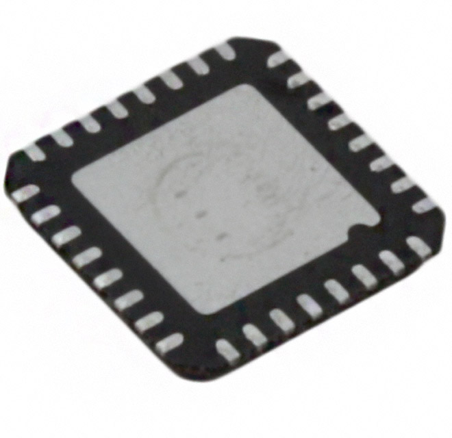
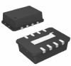
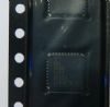
ADL5360: Features: RF Frequency 700MHz to 1000MHzIF Frequency 50MHZ to 350MHzPower Conversion Gain of 8.5dBSSB Noise Figure of 9.5dBSSB NF with +10dBm blocker of 16.5dBInput IP3 of 26dBmInput P1dB of 10 dBmT...
 ADL5360 Data Sheet
floor Price/Ceiling Price
- Part Number:
- ADL5360
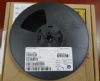
- Supply Ability:
- 5000
Price Break
- Qty
- 1~5000
- Unit Price
- Negotiable
- Processing time
- 15 Days
SeekIC Buyer Protection PLUS - newly updated for 2013!
- Escrow Protection.
- Guaranteed refunds.
- Secure payments.
- Learn more >>
Month Sales
268 Transactions
Payment Methods
All payment methods are secure and covered by SeekIC Buyer Protection PLUS.
Notice: When you place an order, your payment is made to SeekIC and not to your seller. SeekIC only pays the seller after confirming you have received your order. We will also never share your payment details with your seller.