ADL5391

Features: `Ultrafast symmetric multiplier`Function: VW = * (VX * VY)/1 V + VZ`Unique design ensures absolute XY-symmetry`Identical X and Y amplitude/timing responses`Adjustable gain scaling, `DC-coupled throughout, 3 dB bandwidth of 2 GHz`Fully differential inputs, may be used single ended`Low no...

product image

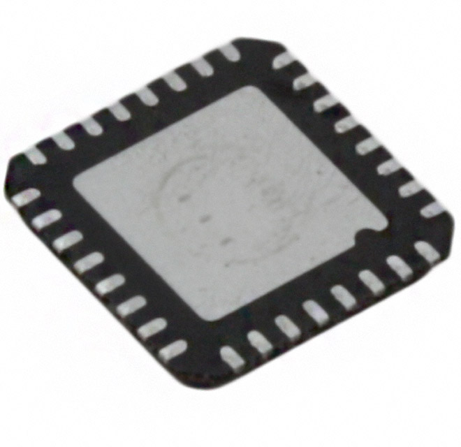
ADL5391 Picture
SeekIC No. : 004275454 Detail

ADL5391: Features: `Ultrafast symmetric multiplier`Function: VW = * (VX * VY)/1 V + VZ`Unique design ensures absolute XY-symmetry`Identical X and Y amplitude/timing responses`Adjustable gain scaling, `DC-co...

floor Price/Ceiling Price

Part Number:
ADL5391
Supply Ability:
5000

Price Break

  • Qty
  • 1~5000
  • Unit Price
  • Negotiable
  • Processing time
  • 15 Days
Total Cost: $ 0.00

SeekIC Buyer Protection PLUS - newly updated for 2013!

  • Escrow Protection.
  • Guaranteed refunds.
  • Secure payments.
  • Learn more >>

Month Sales

268 Transactions

Rating

evaluate  (4.8 stars)

Upload time: 2024/4/30

Payment Methods

All payment methods are secure and covered by SeekIC Buyer Protection PLUS.

Notice: When you place an order, your payment is made to SeekIC and not to your seller. SeekIC only pays the seller after confirming you have received your order. We will also never share your payment details with your seller.
Product Details

Description


Features:

`Ultrafast symmetric multiplier
`Function: VW = * (VX * VY)/1 V + VZ
`Unique design ensures absolute XY-symmetry
`Identical X and Y amplitude/timing responses
`Adjustable gain scaling,
`DC-coupled throughout, 3 dB bandwidth of 2 GHz
`Fully differential inputs, may be used single ended
`Low noise, high linearity
`Accurate, temperature stable gain scaling
`Single-supply operation (4.5 V to 5.5 V @ 130 mA)
`Low current power-down mode
`16-lead LFCSP


Application

·Wideband multiplication and summing
·High frequency analog modulation
·Adaptive antennas (diversity/phased array)
·Square-law detectors and true rms detectors
·Accurate polynomial function synthesis
·DC capable VGA with very fast control


Pinout

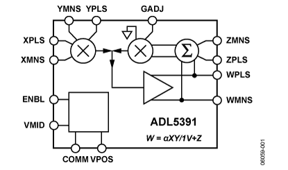
ADL5391 Diagram


Specifications

Supply Voltage VPOS...............5.5 V
ENBL.........................5.5 V
XPLS, XMNS, YPLS, YMNS, ZPLS, ZMNS.... VPOS
GADJ.........................VPOS
Internal Power Dissipation......... 800 mW
JA (With Pad Soldered to Board)..... 73°C/W
Maximum Junction Temperature....... 150°C
Operating Temperature Range..−40°C to +85°C
Storage Temperature Range.. −65°C to +150°C
Lead Temperature (Soldering 60 sec)....300°C


Gain Control Analog
-3 dB BW (MHz) 2000MHz
Gain High End (dB) +9.5dB
Number of Channels 1
Spectral Noise (nV/rtHz) 26.7nV/rtHz
Supply Voltage (V) +5V
Supply Current 135mA


Description

The ADL5391 draws on three decades of experience in advanced analog multiplier products. ADL5391 provides the same general mathematical function that has been field proven to provide an exceptional degree of versatility in function synthesis. VW = * (VX * VY)/ 1 V + VZ

The most significant advance in the ADL5391 is the use of a new multiplier core architecture, which differs markedly from the conventional form that has been in use since 1970. The conventional structure that employs a current mode, translinear core is fundamentally asymmetric with respect to the X and Y inputs, leading to relative amplitude and timing misalignments that are problematic at high frequencies. The new multiplier core eliminates these misalignments by offering symmetric signal paths for both X and Y inputs. The Z input allows a signal to be added directly to the output. This can be used to cancel a carrier or to apply a static offset voltage.

The fully differential X, Y, and Z input interfaces are operational over a ±2 V range, and they can be used in single-ended fashion. The user can apply a common mode at these inputs to vary from the internally set VPOS/2 down to ground. If these inputs are ac-coupled, their nominal voltage will be VPOS/2. These input interfaces each present a differential 500 input impedance up to approximately 700 MHz, decreasing to 50 at 2 GHz. The gain scaling input, GADJ, can be used for fine adjustment of the gain scaling constant () about unity.

The differential output can swing ±2 V about the VPOS/2 common-mode and can be taken in a single-ended fashion as well. The output common mode is designed to interface directly to the inputs of another ADL5391. Light dc loads can be ground referenced; however, ac-coupling of the outputs is recommended for heavy loads.

The ENBL pin allows the ADL5391 to be disabled quickly to a standby mode. It operates off supply voltages from 4.5 V to 5.5 V while consuming approximately 130 mA.

The ADL5391 is fabricated on Analog Devices proprietary, high performance, 65 GHz, SOI complementary, SiGe bipolar IC process. It is available in a 16-lead, Pb-free, LFCSP and operates over a .40°C to +85°C temperature range. Evaluation boards are available.


Customers Who Bought This Item Also Bought

Margin,quality,low-cost products with low minimum orders. Secure your online payments with SeekIC Buyer Protection.
LED Products
Inductors, Coils, Chokes
Programmers, Development Systems
Optical Inspection Equipment
Tapes, Adhesives
803
Semiconductor Modules
View more