Specifications
| -3 dB BW (MHz) |
2900MHz |
| Minimum Gain (Acl) |
6 |
| Supply Current |
40mA |
| Slew Rate (V/us) |
0 |
| Distortion (2nd) (dBc) |
-82dBc |
| Distortion (3rd) (dBc) |
-73dBc |
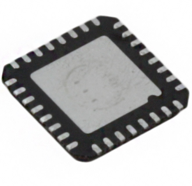
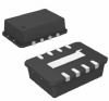
| Package |
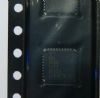
16-Lead LFCSP |
DescriptionThe ADL5561 provides three gain levels of 6 dB, 12 dB, and 15.5 dB through a pin-strappable configuration. For the single-ended input configuration, the gains are reduced to 5.6 dB, 11.1 dB, and 14.1 dB. Using an external series input resistor expands the amplifier gain flexibility and allows for any gain selection from 0 dB to 15.5 dB. The ADL5561 is a high performance differential amplifier optimized for RF and IF applications. The amplifier offers low noise of 2.1 nV/Hz and excellent distortion performance over a wide frequency range, making it an ideal driver for high speed 8-bit to 16-bit analog-to-digital converters (ADCs). This device is optimized for the best combination of slew speed, bandwidth, and broadband distortion. These attributes, together with its adjustable gain capability, make this device the amplifier of choice for general-purpose IF and broadband applications where low distortion, noise, and power are critical. These attributes allow it to drive a wide variety of ADCs and make it ideally suited for driving mixers, pin diode attenuators, SAW filters, and multielement discrete devices. Fabricated on the Analog Devices, Inc., high speed SiGe process, the ADL5561 is supplied in a compact 3 mm * 3 mm, 16-lead LFCSP package and operates over the temperature range of -40°C to +85°C. The quiescent current of the ADL5561 is typically 40 mA and, when disabled, consumes less than 3 mA, offering excellent input-to-output isolation. The device is optimized for wideband, low distortion performance.
The features of ADL5561 can be summarized as (1)-3 dB bandwidth of 2.9 GHz (AV = 6 dB); (2)low supply current: 40 mA; (3)pin-strappable gain adjust: 6 dB, 12 dB, 15.5 dB; (4)differential or single-ended input to differential output; (5)low noise input stage: 2.1 nV/Hz RTI at AV = 12 dB; (6)low broadband distortion (Av = 6 dB)10 MHz: -94 dBc HD2, -87 dBc HD3/ 70 MHz: -98 dBc HD2, -87 dBc HD3/ 140 MHz: -95 dBc HD2, -87 dBc HD3/ 250 MHz: -80 dBc HD2, -73 dBc HD3; (7)IMD3s of -86 dBc @ 250 MHz center; (8)slew rate: 9.8 V/ns; (9)fast settling of 2 ns and overdrive recovery of 3 ns; (10)single-supply operation: 3 V to 3.6 V; (11)power-down control; (12)fabricated using the high speed XFCB3 SiGe process.
The absolute maximum ratings of ADL5561 are (1)supply voltage (VCC): 3.6 V; (2)VIP1, VIP2, VIN1, VIN2: VCC + 0.5 V; (3)internal power dissipation: 155 mW; (4)JA 98.3°C/W; (5)maximum junction temperature: 125°C; (6)operating temperature range: -40°C to +85°C; (7)storage temperature range: -65°C to +150°C.

 ADL5561 Data Sheet