Features: Monitoring of 12 V, 5 V, 3.3 V and 2.8 V Supplies in Parallel
Auxiliary Sensor Inputs
Low Power: 25A Typical
Internal Comparator Hysteresis
Power Supply Glitch Immunity
VCC from 2.5 V to 6 V
Guaranteed from 40C to +85C
No External Components
16-Pin Narrow SOIC Package (150 Mil Wide)ApplicationA typical application of the ADM9264 is shown in Figure 23. The analog inputs SU1 to SU4 are connected to the four power supply outputs of a system to monitor the supply voltages. One of the digital inputs, ERRY, is connected to a temperature sensor such as the TMP01 or AD22105. The trip point of the overtemperature comparator is set by RSET so that the output goes low when the temperature exceeds safe limits. (See the appropriate Analog Devices data sheet for more information on these devices.)
The other digital input, ERRX, is connected to a fan failure sensor. This can be something as simple as a vane switch
mounted in the fan air flow, which opens if the air flow fails.
The digital outputs of the ADM9264 are interfaced to the system microprocessor through the GPIO lines or via an I/O adapter chip. Depending on the level of fault diagnostics required in the system, the four error outputs (ERR1 to ERR4) corresponding to the analog inputs SU1 to SU4 can be individually connected to the I/O chip to give specific indication of which supply voltage has failed, while the PWROK output indicates an overtemperature or system cooling failure. Alternatively, the PWROK output can be used alone to give a nonspecific failure indication.
Pinout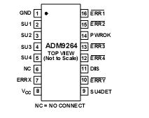
 Specifications
(TA = +25°C unless otherwise noted) VCC . . . . . . . . . . . . . . . . . . . . . . . . . . . . . . . . . 0.3 V to +6 V SU1, SU2, SU3, SU4 . . . . . . . . . . . . . . . . . . 0.3 V to +15 V All Other Inputs . . . . . . . . . . . . . . . . . . 0.3 V to VCC + 0.3 V All Outputs . . . . . . . . . . . . . . . . . . . . . . . . . . . 0.3 V to +6 V Output Current ERR1-4, PWROK . . . . . . . . . . . . . . . . 20 mA Operating Temperature Range Industrial (A Version) . . . . . . . . . . . . . . . . 40°C to +85°C Power Dissipation, R-16A . . . . . . . . . . . . . . . . . . . 700 mW JA Thermal Impedance . . . . . . . . . . . . . . . . . . . 110°C/W Lead Temperature (Soldering, 10 secs) . . . . . . . . . . . . +300°C Vapor Phase (60 secs) . . . . . . . . . . . . . . . . . . . . . . . +215°C Infrared (15 secs) . . . . . . . . . . . . . . . . . . . . . . . . . . . +220°C Storage Temperature Range . . . . . . . . . . . . 65°C to +150°C *Stresses above those listed under Absolute Maximum Ratings may cause permanent damage to the device. This is a stress rating only; functional operation of the device at these or any other conditions above those listed in the operational sections of this specification is not implied. Exposure to absolute maximum ratings for extended periods of time may affect device reliability.
| # of Monitored Voltages |
4 |
| Manual Reset Capability |
No |
| Package |
SOIC |
| Reset Threshold Summary |
4 Options--2.6 to 11.04V |
| Reset Output-Stage |
Active-Low/Open-Drain |
| Min Reset Timeout (ms) |
n/a |
| Typ Watchdog Timeout (ms) |
--- |
DescriptionThe ADM9264 is a Quad Supply Monitor IC which simultaneously monitors four separate power supply voltages and outputs error signals if any of the supply voltages go out of limits. ADM9264 is designed for PC supply monitoring but can be used on any system where multiple power supplies require monitoring. The error output signals are available individually and also gated into a common output - PWROK. Auxiliary inputs ERRX, ERRY are provided which are also gated into the main PWROK signal. These inputs allow signals from other monitoring circuits (for example temperature sensor, alarm, etc.) to be inked into the ADM9264. Each power supply monitor circuit of ADM9264 uses a proprietary window comparator design whereby a three resistor network is used in conjunction with two comparators and a single precision voltage reference to check if the supply is within its required operating tolerance. An added feature of this design is that the power supply voltages being monitored can be higher than the power supply voltage to the monitoring IC itself. Analog Devices' experience in the design of power supply supervisory circuits is used to provide an optimum solution for the overall circuit in terms of cost, performance and power consumption. Key features of the design include the incorporation of hysteresis and glitch immunity into the comparators, which minimizes the possibility of spurious triggering by noise spikes on the supplies being monitored. The part of ADM9264 is manufactured on one of Analog Devices' proprietary BiCMOS processes, which also includes high performance thin film resistors to achieve the accuracy required for the precision voltage reference and power supply high and low trip points.

 ADM9264 Data Sheet


