ADN2811

Features: Meets SONET Requirements for Jitter Transfer/Generation/ToleranceQuantizer Sensitivity: 4 mV Typ1.9 GHz Minimum BandwidthPatented Clock Recovery ArchitectureLoss of Signal Detect Range: 3 mV to 15 mVSingle Reference Clock Frequency for Both Native SONET and 15/14 (7%) Wrapper RateChoice ...

product image

ADN2811 Picture
SeekIC No. : 004276175 Detail

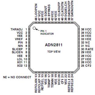
ADN2811: Features: Meets SONET Requirements for Jitter Transfer/Generation/ToleranceQuantizer Sensitivity: 4 mV Typ1.9 GHz Minimum BandwidthPatented Clock Recovery ArchitectureLoss of Signal Detect Range: 3 ...

floor Price/Ceiling Price

Part Number:
ADN2811
Supply Ability:
5000

Price Break

  • Qty
  • 1~5000
  • Unit Price
  • Negotiable
  • Processing time
  • 15 Days
Total Cost: $ 0.00

SeekIC Buyer Protection PLUS - newly updated for 2013!

  • Escrow Protection.
  • Guaranteed refunds.
  • Secure payments.
  • Learn more >>

Month Sales

268 Transactions

Rating

evaluate  (4.8 stars)

Upload time: 2024/4/28

Payment Methods

All payment methods are secure and covered by SeekIC Buyer Protection PLUS.

Notice: When you place an order, your payment is made to SeekIC and not to your seller. SeekIC only pays the seller after confirming you have received your order. We will also never share your payment details with your seller.
Product Details

Description


Features:

Meets SONET Requirements for Jitter Transfer/Generation/Tolerance
Quantizer Sensitivity: 4 mV Typ
1.9 GHz Minimum Bandwidth
Patented Clock Recovery Architecture
Loss of Signal Detect Range: 3 mV to 15 mV
Single Reference Clock Frequency for Both Native SONET and 15/14 (7%) Wrapper Rate
Choice of 19.44 MHz, 38.88 MHz, 77.76 MHz, or 155.52 MHz
  REFCLK LVPECL/LVDS/LVCMOS/LVTTL
  Compatible Inputs (LVPECL/LVDS Only at 155.52 MHz)
  19.44 MHz Oscillator On-Chip to Be Used with
  External Crystal
Loss of Lock Indicator
Loopback Mode for High Speed Test Data
Output Squelch and Bypass Features
Single-Supply Operation: 3.3 V
Low Power: 540 mW Typical


Application

SONET OC-48, SDH STM-16, and 15/14 FEC
WDM Transponders
Regenerators/Repeaters
Test Equipment
Backplane Applications


Pinout

  Connection Diagram


Specifications

Supply Voltage (VCC)  . . . . . . . . . . . . . . . . . . . . . . . . . . 5.5 V
Minimum Input Voltage (All Inputs)  . . . . . . . . . .  VEE 0.4 V
Maximum Input Voltage (All Inputs)  . . . . . . . .    VCC + 0.4 V
Maximum Junction Temperature  . . . . . . . . . . . . . . . . .  165
Storage Temperature  . . . . . . . . . . . . . . . . . 65 to +150
Lead Temperature (Soldering 10 Sec)  . . . . . . . . . . . . . 300


Description

The ADN2811 provides the receiver functions of quantization, signal level detect, and clock and data recovery at OC-48 and OC-48 FEC rates. All SONET jitter requirements are met, including jitter transfer, jitter generation, and jitter tolerance. All specifications are quoted for 40C to +85C ambient temperature, unless otherwise noted. The device is intended for WDM system applications and can be used with either an external reference clock or an on-chip oscillator with external crystal. Both the 2.48 Gb/s and 2.66 Gb/s digital wrapper rate is supported by the ADN2811, without any change of reference clock.

This device, together with a PIN diode and a TIA preamplifier, can implement a highly integrated, low cost, low power, fiber optic receiver. The receiver front end signal detect circuit indicates when the input signal level has fallen below a user-adjustable threshold. The signal detect circuit has hysteresis to prevent chatter at the output. The ADN2811 is available in a compact 7 mm *   7 mm 48-lead chip scale package.


Customers Who Bought This Item Also Bought

Margin,quality,low-cost products with low minimum orders. Secure your online payments with SeekIC Buyer Protection.
LED Products
Optoelectronics
Discrete Semiconductor Products
Batteries, Chargers, Holders
Sensors, Transducers
Motors, Solenoids, Driver Boards/Modules
View more