ADP3050

Features: Wide Input Voltage Range: 3.6 V to 30 VAdjustable and Fixed (3.3 V, 5 V) Output OptionsIntegrated 1 A Power SwitchUses Small Surface-Mount ComponentsCycle-By-Cycle Current LimitingPeak Input Voltage (100 ms): 60 VThermally Enhanced 8-Lead SOIC PackageConfigurable as a Buck, Buck-Boost an...

product image

ADP3050 Picture
SeekIC No. : 004276421 Detail

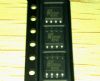
ADP3050: Features: Wide Input Voltage Range: 3.6 V to 30 VAdjustable and Fixed (3.3 V, 5 V) Output OptionsIntegrated 1 A Power SwitchUses Small Surface-Mount ComponentsCycle-By-Cycle Current LimitingPeak Inp...

floor Price/Ceiling Price

Part Number:
ADP3050
Supply Ability:
5000

Price Break

  • Qty
  • 1~5000
  • Unit Price
  • Negotiable
  • Processing time
  • 15 Days
Total Cost: $ 0.00

SeekIC Buyer Protection PLUS - newly updated for 2013!

  • Escrow Protection.
  • Guaranteed refunds.
  • Secure payments.
  • Learn more >>

Month Sales

268 Transactions

Rating

evaluate  (4.8 stars)

Upload time: 2024/4/30

Payment Methods

All payment methods are secure and covered by SeekIC Buyer Protection PLUS.

Notice: When you place an order, your payment is made to SeekIC and not to your seller. SeekIC only pays the seller after confirming you have received your order. We will also never share your payment details with your seller.
Product Details

Description


Features:

Wide Input Voltage Range: 3.6 V to 30 V
Adjustable and Fixed (3.3 V, 5 V) Output Options
Integrated 1 A Power Switch
Uses Small Surface-Mount Components
Cycle-By-Cycle Current Limiting
Peak Input Voltage (100 ms): 60 V
Thermally Enhanced 8-Lead SOIC Package
Configurable as a Buck, Buck-Boost and SEPIC
Regulator


Application

Industrial Power Systems
PC Peripheral Power Systems
Preregulator for Linear Regulators
Distributed Power Systems
Automotive Systems
Battery Chargers


Pinout

  Connection Diagram


Specifications

IN Voltage
Steady State . . . . . . . . . . . . . . . . . . . . . . . . . . . . . .0.3 V to +30 V
Peak (<100 ms) . . . . . . . . . . . . . . . . . . . . . . . . . . . 0.3 V to +60 V
BOOST Voltage
Steady State . . . . . . . . . . . . . . . . . . . . . . . . . . . . . 0.3 V to +45 V
Peak (<100 ms) . . . . . . . . . . . . . . . . . . . . . . . . . . . 0.3 V to +65 V
SD, BIAS Voltage . . . . . . . . . . . . . . . . . . . . . . . 0.3 V to IN + 0.3 V
FB Voltage . . . . . . . . . . . . . . . . . . . . . . . . . . . . . . . . 0.3 V to +8 V
COMP Voltage . . . . . . . . . . . . . . . . . . . . . . . . . 0.3 V to IN + 0.3 V
SWITCH Voltage . . . . . . . . . . . . . . . . . . . . . . . 0.3 V to IN + 0.3 V
Operating Ambient Temperature Range . . . . . . . . 40°C to +85°C
Operating Junction Temperature Range . . . . . . . 40°C to +125°C
Storage Temperature Range . . . . . . . . . . . . . . . .65°C to +150°C
JA (2-Layer PCB) . . . . . . . . . . . . . . . . . . . . . . . . . . . . . . .108°C/W
JA (4-Layer PCB) . . . . . . . . . . . . . . . . . . . . . . . . . . . . . . . .81°C/W
Lead Temperature Range (Soldering, 60 sec.) . . . . . . . . . . . 300°C
*This is a stress rating only; operation beyond these limits can cause the device to be permanently damaged. Unless otherwise specified, all voltages are referenced to GND


Description

The ADP3050 is a current-mode monolithic buck (step-down) PWM switching regulator that contains a high current 1 A power switch and all control, logic, and protection functions. It uses a unique compensation scheme that allows the use of any type of output capacitor (tantalum, ceramic, electrolytic, OS-CON). Unlike some buck regulators, the design is not restricted to using a specific type of output capacitor or ESR value.

A special boosted drive stage is used to saturate the NPN power switch, providing a system efficiency higher than conventional bipolar buck switchers. Further efficiency improvements are obtained by using the low voltage regulated output to provide the device's internal operating current. A high switching frequency allows the use of small external surface-mount components. A wide variety of standard off-the-shelf devices can be used, providing a great deal of design flexibility. A complete regulator design of ADP3050 requires only a few external components.

The ADP3050 includes a shutdown input that places the device in a low-power mode, reducing the total supply current to under 20 A. Internal protection features include thermal shutdown circuitry and a cycle-by-cycle current-limit for the power switch to provide complete device protection under fault conditions.

The ADP3050 provides excellent line and load regulation, maintaining typically less than ±3% output voltage accuracy over temperature and under all input voltage and output current conditions.

The ADP3050 is specified over the industrial temperature range of 40°C to +85°C and is available in a thermally enhanced 8-lead SOIC package.


Customers Who Bought This Item Also Bought

Margin,quality,low-cost products with low minimum orders. Secure your online payments with SeekIC Buyer Protection.
Line Protection, Backups
RF and RFID
Tapes, Adhesives
803
Boxes, Enclosures, Racks
View more