ADS5102

Features: ADS5102 (65 MSPS) ADS5103 (40 MSPS) Differential Input 1.8 V Analog/Digital Supply Digital Outputs Compatible With 1.8 V or 3.3 V Logic Signal-to-Noise: 58 dB at 20 MHz (ADS5103) Spurious Free Dynamic Range: 71 dB at 20 MHz (ADS5102) 105-mW Power Dissipation (ADS5103) 336 µW Power...

product image

ADS5102 Picture
SeekIC No. : 004277135 Detail

ADS5102: Features: ADS5102 (65 MSPS) ADS5103 (40 MSPS) Differential Input 1.8 V Analog/Digital Supply Digital Outputs Compatible With 1.8 V or 3.3 V Logic Signal-to-Noise: 58 dB at 20 MHz (ADS5103) Spurious...

floor Price/Ceiling Price

Part Number:
ADS5102
Supply Ability:
5000

Price Break

  • Qty
  • 1~5000
  • Unit Price
  • Negotiable
  • Processing time
  • 15 Days
Total Cost: $ 0.00

SeekIC Buyer Protection PLUS - newly updated for 2013!

  • Escrow Protection.
  • Guaranteed refunds.
  • Secure payments.
  • Learn more >>

Month Sales

268 Transactions

Rating

evaluate  (4.8 stars)

Upload time: 2024/4/28

Payment Methods

All payment methods are secure and covered by SeekIC Buyer Protection PLUS.

Notice: When you place an order, your payment is made to SeekIC and not to your seller. SeekIC only pays the seller after confirming you have received your order. We will also never share your payment details with your seller.
Product Details

Description


Features:

ADS5102 (65 MSPS) ADS5103 (40 MSPS)
Differential Input
1.8 V Analog/Digital Supply
Digital Outputs Compatible With 1.8 V or 3.3 V Logic
Signal-to-Noise: 58 dB at 20 MHz (ADS5103)
Spurious Free Dynamic Range: 71 dB at 20 MHz (ADS5102)
105-mW Power Dissipation (ADS5103)
336 µW Power-Down Mode


Application

Ultrasound
Digital Cameras
Imaging
Communications
Baseband Digitization


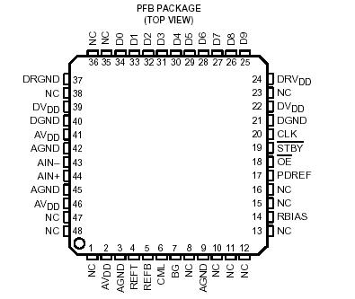
Pinout

  Connection Diagram


Specifications

TERMINAL

NAME NO.

I/O DESCRIPTION
AVDD 2, 41, 46 I Analog supply, 1.8V ±5%
AGND 3, 9, 42, 45 I Analog ground
REFT 4 I/O Reference top
REFB 5 I/O Reference bottom
CML 6 O Common mode level output-nominally 1.0 V
BG 7 O Band-gap decoupling-decouple with 1 µF to GND and 100 kΩ to AVDD (refer to Figure 30)
PDREF 17 I Powerdown reference when using external voltage reference 0 = internal VREF, 1 = external VREF.
In external VREF mode, connect pins BG and REFT together.
RBIAS 14 O Connect a resistor between this pin and AGND. This resistor value is determined by speed grade
selected and is used to set amplifier internal bias currents. (see Table 2)
OE 18 I 1 = 3-state the data outputs , 0 = data bus enable
STBY 19 I 0 = power down mode, 1 = normal operation mode
CLK 20 I Clock Input
DGND 21, 40 I Digital ground
DVDD 22, 39 I Digital supply-1.8 V nominally
DRVDD 24 I Driver digital supply-1.8 V or 3.3 V nominally
D9 25 O Digital Bit 9 (MSB)
D8 26 O Digital Bit 8
D7 27 O Digital Bit 7
D6 28 O Digital Bit 6
D5 29 O Digital Bit 5
D4 30 O Digital Bit 4
D3 31 O Digital Bit 3
D2 32 O Digital Bit 2
D1 33 O Digital Bit 1
D0 34 O Digital Bit 0
DRGND 37 I Driver digital ground
AIN+ 44 I Positive analog input
AIN 43 I Negative analog input
NC

1,8,10,11,12,
13,15,16,23,35,
36, 38,47,48

NA No internal connection on this pin


Description

The ADS5102/3 are low-power CMOS, 10-bit, analogto- digital converters (ADC) that operate from a single 1.8-V supply. The internal reference can be bypassed to use an external reference to suit the dc accuracy and temperature drift requirements of the application. A 10-bit parallel output data bus is provided with 3-state outputs. For power sensitive systems, a standby mode is provided which reduces power consumption to 336 µW. Also, if using external voltage reference, then the internal VREF circuit can be powered down. The analog input is differential, which provides excellent common-mode noise rejection as well as superior performance from the ADS5102/3.


Customers Who Bought This Item Also Bought

Margin,quality,low-cost products with low minimum orders. Secure your online payments with SeekIC Buyer Protection.
Line Protection, Backups
Tapes, Adhesives
803
Fans, Thermal Management
Memory Cards, Modules
Test Equipment
View more