Features: ` 320 MIPS ADSP-219x DSP in a 144-Lead LQFP Package with PCI, USB, Sub-ISA, and CardBus Interfaces
` 3.3 V/5.0 V PCI 2.2 Compliant 33 MHz/32-bit Interface with Bus Mastering over Four DMA Channels with Scatter-ather Support
` Integrated USB 1.1 Compliant Interface
` Sub-ISA Interface
` AC'97 Revision 2.1 Compliant Interface for External
Audio, Modem, and Handset Codecs with DMA Capability
` Dual ADSP-219x Core Processors (P0 and P1) on Each ADSP-2192M DSP Chip
` 132K Words of Memory Includes 4K *16-Bit Shared Data Memory
` 80K Words of On-Chip RAM on P0, Configured as
64K Words On-Chip 16-Bit RAM for Data Memory and
16K Words On-Chip 24-Bit RAM for Program Memory
` 48K Words of On-Chip RAM on P1, Configured as
32K Words On-Chip 16-Bit RAM for Data Memory and
16K Words On-Chip 24-Bit RAM for Program Memory
` 4K Words of Additional On-Chip RAM Shared by Both Cores, Configured as 4K Words On-Chip 16-Bit RAM
` Flexible Power Management with Selectable Power-Down and Idle Modes
` Programmable PLL Supports Frequency Multiplication,Enabling Full Speed Operation from Low Speed Input Clocks
` 2.5 V Internal Operation Supports 3.3 V/5.0 V Compliant I/O ` Eight Dedicated General-Purpose I/O Pins with Integrated Interrupt Support
` Each DSP Core Has a Programmable 32-Bit Interval Timer
` Five DMA Channels Available on Each Core
` Boot Methods Include Booting Through PCI Port, USB Port, or Serial EEPROM
` JTAG Test Access Port Supports On-Chip Emulation and System Debugging
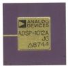
` 144-Lead LQFP Package
SpecificationsPower Supply, Internal (VDDINT)1 . . . . . . .. 0.3 V to +6.0 V
Power Supply, External (VDDEXT) . . . . . . ... 0.3 V to +6.0 V
Input Voltage (Signal Pins) . . . . . . 0.3 V to VDDEXT + 0.3 V
TSTORE Storage Temperature Range . . . . 65ºC to +150ºC
TLEAD Lead Temperature (5 seconds) max . . . . . . . . 185ºC
1Stresses greater than those listed above may cause permanent damage to the device. These are stress ratings only; functional operation of the device at these or any other conditions greater than those indicated in the operational sections of this specification is not implied. Exposure to absolute maximum rating conditions for extended periods may affect device reliability.
DescriptionThe ADSP-2192M is a single-chip microcomputer optimized for digital signal processing (DSP) and other high speed numeric processing applications, and is ideally suited for PC peripherals.
The ADSP-2192M combines the ADSP-219x family base architecture (three computational units, two data address generators and a program sequencer) into a chip with two core processors (see the Functional Block Diagram on Page 1 and Figure 1).
The ADSP-2192M includes a PCI-compatible port, a USBcompatible port, an AC'97-compatible port, a DMA controller, a programmable timer, general-purpose Programmable Flag pins, extensive interrupt capabilities, and on-chip program and data memory spaces.
The ADSP-2192M integrates 132K words of on-chip memory configured as 32K words (24-bit) of program RAM, and 100K words (16-bit) of data RAM. power-down circuitry is also provided to reduce power consumption. The ADSP-2192M is available in a 144-lead LQFP package.
Fabricated in a high speed, low power, CMOS process, the ADSP-2192M operates with a 6.25 ns instruction cycle time (320 MIPS) using both cores. All instructions can execute in a single DSP cycle.
The ADSP-2192M's flexible architecture and comprehensive instruction set support multiple operations in parallel. For example, in one processor cycle, each DSP core within the product can:
• Generate an address for the next instruction fetch
• Fetch the next instruction
• Perform one or two data moves
• Update one or two data address pointers
• Perform a computational operation
These operations take place while the processor continues to:
• Receive and/or transmit data through the Host port (PCI or USB interfaces)
• Receive or transmit data through the AC'97
• Decrement the two timers

 ADSP-2192M Data Sheet