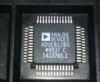
Pinout Description
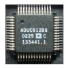
The ADuC812 is a fully integrated 12-bit data acquisition system with a high performance self-calibrating multichan nel ADC, two 12-bit DACs and programmable 8-bit(8051-compatible) MCU on a single chip.The programmable 8051-compatible core is supported by 8K bytes Flash/EE program memory, 640 bytes Flash/EE data memory and 256 bytes data SRAM on-chip.Additional MCU support functions are consisted of Watchdog Timer, Power Supply Monitor and ADC DMA functions. 32 Programmable I/O lines, I2C-compatible, SPI and Standard UART Serial Port I/O are offer ed for multiprocessor interfaces and I/O expansion.Normal, idle and power-down operating modes for both the MCU core and analog converters accept flexible power management schemes applied to low power applications.
The ADuC812 has the following features:(1):ANALOG I/O:8-Channel, high accuracy 12-Bit ADC,on-chip, 40 ppm/�C voltage reference,high speed 200 kSPS,DMA controller for high speed ADC-to-RAM capture,two 12-bit voltage output DACs,on-chip temperature sensor function;(2)memory:8K bytes on-chip flash/ee program memory,640 bytes on-chip flash/EE data memory,on-chip charge pump (No Ext. VPP requirements),256 bytes on-chip data RAM,16M bytes external data address space,64K bytes external program address space(3)8051-COMPATIBLE CORE:12 MHz nominal operation (16 MHz Max),three 16-bit timer/counters,32 programmable I/O lines,high current drive capability-Port 3,nine interrupt sources, two priority levels(4)power:specified for 3 V and 5 V operation,normal, idle and power-do wn modes.etc
ADuC812 also has some outstanding absolute maximum ratings(Ta=25°C) and specifications:(1)AVDD to DVDD ranges fro m0.3 V to +0.3 V;(2)AGND to DGND ranges from0.3 V to +0.3 V;(3):DVDD to DGND, AVDD to AGND ranges from0.3 V to +7 V;(4)Digital Input Voltage to DGND ranges from 0.3 V to DVDD + 0.3 V;(5)Digital Output Voltage to DGN D ranges from0.3 V to DVDD + 0.3 V;(6):VREF to AGND ranges from0.3 V to AVDD + 0.3 V;(7):Analog Inputs to AGND ranges from0.3 V to AVDD + 0.3 V;(8):Operating Temperature Ranges from40°C to +85°C, Storage Tem perature Ranges from65°C to +150°C.specifications:(1):resolution is 12 bit when VDD is 5V;(2):Integral Nonli nearity is±1/2 LSB typ when fSAMPLE is 100 kHz and VDD is 5V;(3):differential nonlinearity is±1 LSB typ when fSAMP LE is 100 kHz;(4):offset error is±5 LSB max when VDD is 5V;(5):offset error match is 1 LSB typ when VDD is 5V;(6)offset calibration range is ±5 % of VREF typ when VDD is 5V;(7):Resolution 12 bits when VDD is 5V.etc.
Parameters: | Technical/Catalog Information | ADUC812BS |
| Vendor | Analog Devices Inc |
| Category | Integrated Circuits (ICs) |
| Program Memory Size | 8K x 8 |
| RAM Size | 256 x 8 |
| Number of I /O | 34 |
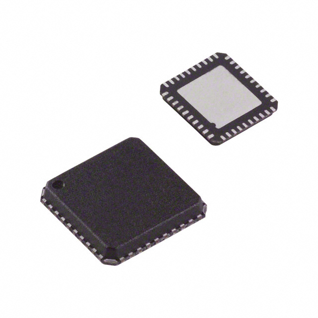
| Package / Case | 52-MQFP, 52-PQFP |
| Speed | 16MHz |
| Controller Series | ADuC8xx |
| Oscillator Type | Internal |
| Packaging | Tray |
| Program Memory Type | FLASH |
| EEPROM Size | 640 x 8 |
| Core Processor | 8052 |
| Data Converters | A/D 8x12b; D/A 2x12b |
| Core Size | 8-Bit |
| Operating Temperature | -40°C ~ 85°C |
| Connectivity | I²C, SPI, UART/USART |
| Peripherals | PSM, Temp Sensor, WDT |
| Voltage - Supply (Vcc/Vdd) | 2.7 V ~ 5.5 V |
| RoHS Status | RoHS Non-Compliant |
| Other Names | ADUC812BS
ADUC812BS
|

 ADUC812BS Data Sheet