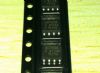
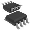
Pinout Specifications
| Max Operating Temp (°C) |
85Deg |
| Insulation Rating (kVrms) |
2.5kV rms |
| # Ch |
2 |
| Pulse Width Distort (ns) |
3ns |
| Max Prop Delay (ns) |
45ns |
| Isolated Output (V)min |
2.7V |
| Isolated Output (V)max |
5.5V |
| Output Default State |
High |
DescriptionThe ADUM3201 are dual-channel, digital isolators based on the Analog Devices, Inc.
iCoupler? technology. Combining high speed CMOS and monolithic transformer technology, these isolation
The ADUM3201 is dual-channel, digital isolator based on analog devices' icoupler® technology.Combining high speed CMOS and monolithic transformer technology, the isolation component provides outstanding performance characteristics superior to alternatives such as optocoupler devices.
Features of the ADUM3201 are:(1)enhanced system-level ESD performance per IEC 61000-4-x;(2)narrow body, 8-lead SOIC, Pb-free package;(3)bidirectional communication;(4)3 V/5 V level translation;(5)high temperature operation: 105;(6)high data rate: dc to 25 Mbps (NRZ);(7)high common-mode transient immunity: >25 kV/s;(8)UL recognition: 2500 V rms for 1 minute per UL 1577;(9)CSA component acceptance notice #5A.By avoiding the use of LEDs and photodiodes, iCoupler devices remove the design difficulties commonly associated with optocouplers. The typical optocoupler concerns regarding uncertain current transfer ratios, nonlinear transfer functions, and temperature and lifetime effects are eliminated with the simple iCoupler digital interfaces and stable performance characteristics.
The absolute maximum ratings of the ADUM3201 can be summarized as:(1)supply voltages:-0.5 to +7.0 V;(2)storage temperature:-55 to +150;(3)input voltage:-0.5 to VDDI+0.5V;(4)ambient operating temperature:40 to +105;(5)output voltage:-0.5 to VDDO + 0.5 V;(6)average output current, per pin:-35 to 35mA.Stresses above those listed under Absolute Maximum Ratings may cause permanent damage to the device. This is a stress rating only; Functional operation of the device at these or any other conditions above those listed in the operational sections of this specification is not implied. Exposure to absolute maximum rating conditions for extended periods may affect device reliability.Positive and negative logic transitions at the isolator input cause narrow (~1 ns) pulses to be sent to the decoder via the transformer. The decoder is bistable and is therefore either set or reset by the pulses, indicating input logic transitions. In the absence of logic transitions of more than 2 s at the input, a periodic set of refresh pulses indicative of the correct input state are sent to ensure dc correctness at the output. If the decoder receives no internal pulses for more than about 5 s, the input side is assumed to be unpowered or nonfunctional, in which case, the isolator output is forced to a default state (see Table 8) by the watchdog timer circuit.

 ADUM3201 Data Sheet