Features: High-Resolution Sigma-Delta ADCs
Dual 16-Bit Independent ADCs
Programmable Gain Front End
16-Bit No Missing Codes, Primary ADC
13-Bit p-p Resolution @ 20 Hz, 20 mV Range
16-Bit p-p Resolution @ 20 Hz, 2.56 V Range
Memory
8 Kbytes On-Chip Flash/EE Program Memory
640 Bytes On-Chip Flash/EE Data Memory
Flash/EE, 100 Year Retention, 100 Kcycles Endurance
256 Bytes On-Chip Data RAM
8051-Based Core
8051-Compatible Instruction Set (12.58 MHz Max)
32 kHz External Crystal, On-Chip Programmable PLL
Three 16-Bit Timer/Counters
26 Programmable I/O Lines
11 Interrupt Sources, Two Priority Levels
Power
Specified for 3 V and 5 V Operation
Normal: 3 mA @ 3 V (Core CLK = 1.5 MHz)
Power-Down: 20 �A (32 kHz Crystal Running)
On-Chip Peripherals
On-Chip Temperature Sensor
12-Bit Voltage Output DAC
Dual Excitation Current Sources
Reference Detect Circuit
Time Interval Counter (TIC)
UART Serial I/O
I2C®-Compatible and SPI® Serial I/O
Watchdog Timer (WDT), Power Supply Monitor (PSM)ApplicationIntelligent Sensors (IEEE1451.2-Compatible)
Weigh Scales
Portable Instrumentation
Pressure Transducers
420 mA TransmittersPinout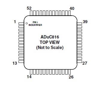 SpecificationsAVDD to AGND . . . . . . . . . . . . . . . . ................................... . . . . . . 0.3 V to +7 V
AVDD to DGND . . . . . . . . . . . . . . . . ................................... . . . . . . 0.3 V to +7 V
DVDD to AGND . . . . . . . . . . . . . . . . . ................................... . . . . . 0.3 V to +7 V
DVDD to DGND . . . . . . . . . . . . . . . . . . . ................................... . . . 0.3 V to +7 V
AGND to DGND2 . . . . . . . . . . . . . . . . . ...................................... . 0.3 V to +0.3 V
AVDD to DVDD . . . . . . . . . . . . . . . . . . ................................... . . . . . . 2 V to +5 V
Analog Input Voltage to AGND3 . . . .................................. 0.3 V to AVDD +0.3 V
Reference Input Voltage to AGND ................................... . 0.3 V to AVDD +0.3 V
AIN/REFIN Current (Indefinite) . . . ..................................... . . . . . . . . . . . . 30 mA
Digital Input Voltage to DGND . . . .................................... 0.3 V to DVDD +0.3 V
Digital Output Voltage to DGND . . .................................... 0.3 V to DVDD +0.3 V
Operating Temperature Range . . . . . . . . ............................... . . 40°C to +85°C
Storage Temperature Range . . . . . . . . . . . . .............................65°C to +150°C
Junction Temperature . . . . . . . . . . . . . . . . . . . . ................................ . . . . 150°C
JA Thermal Impedance . . . . . . . . . . . . . . . . . . . . . .............................. . 90°C/W
Lead Temperature, Soldering
Vapor Phase (60 sec) . . . . . . . . . . . . . . . . . . . . . .............................. . . 215°C
Infrared (15 sec) . . . . . . . . . . . . . . . . . . . . . . . . . ................................ . 220°CDescriptionThe ADuC816 is a complete smart transducer front-end, integrating two high-resolution sigma-delta ADCs, an 8-bit MCU, and program/data Flash/EE Memory on a single chip. This low power device accepts low-level signals directly from a transducer.
The two independent ADCs (Primary and Auxiliary) include a temperature sensor and a PGA (allowing direct measurement of
low-level signals). The ADCs with on-chip digital filtering are intended for the measurement of wide dynamic range, low frequency signals, such as those in weigh scale, strain gauge, pressure transducer, or temperature measurement applications. The ADC output data rates are programmable and the ADuC816 ADC output resolution will vary with the programmed gain and output rate.
The device operates from a 32 kHz crystal with an on-chip PLL generating a high-frequency clock of 12.58 MHz. This clock is, in turn, routed through a programmable clock divider from which the MCU core clock operating frequency is generated. The microcontroller core is an 8052 and therefore 8051-instructionset- compatible. The microcontroller core machine cycle consists of 12 core clock periods of the selected core operating frequency. 8 Kbytes of nonvolatile Flash/EE program memory are provided on-chip. 640 bytes of nonvolatile Flash/EE data memory and 256 bytes RAM are also integrated on-chip.
The ADuC816 also incorporates additional analog functionality with a 12-bit DAC, current sources, power supply monitor, and a bandgap reference. On-chip digital peripherals include a watchdog timer, time interval counter, three timers/counters, and three serial I/O ports (SPI, UART, and I2C-compatible).
On-chip factory firmware supports in-circuit serial download and debug modes (via UART), as well as single-pin emulation mode via the EA pin. A functional block diagram of the ADuC816 is shown above with a more detailed block diagram shown in Figure 12.
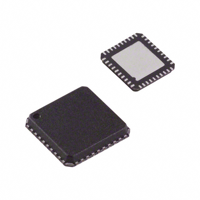
The part operates from a single 3 V or 5 V supply. When operating from 3 V supplies, the power dissipation for the part is below 10 mW. The ADuC816 is housed in a 52-lead MQFP package.

 ADuC81 Data Sheet