Features: ` Switching Rates up to 32 MHz
` Operates from a Single 3.3-V Supply
` Ultra-Low Power Dissipation . . . 27 mW Typ
` Open-Circuit, Short-Circuit, and Terminated Fail-Safe
` 0.3-V to 5.5-V Common-Mode Range With ±200 mV Sensitivity
` Accepts 5-V Logic Inputs With a 3.3-V VCC
` Input Hysteresis . . . 50 mV Typ
` 235 mW With Four Receivers at 32 MHz
` Pin-to-Pin Compatible With AM26C32,AM26LS32, and MB570Pinout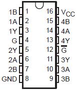 Specifications
Supply voltage range, VCC (see Note 1) . . . . . . . . . . . .. . . . . 0.3 V to 6 V
Input voltage range, VI (A or B inputs) . . . . . . . . . . . . . . . . . . .. 4 V to 8 V
Differential input voltage, VID (see Note 2) . . . . . . . . . . . . . . . . . . . . ±12 V
Enable input voltage range . . . . . . . . . . . . . . . . . . . .. . . . . . ..0.3 V to 6 V
Output voltage range, VO . . . . . . . . . . . . . . . . . . . ... . . . . . . 0.3 V to 6 V
Maximum output current, IO . . . . . . . . . . . . . . . . . . . . . . . . . . . . . ..±25 mA
Package thermal impedance, JA (see Note 3): D package . .. . . ...73°C/W
NS package . . . . . . . . . . . . . . . . . . ...64°C/W
Lead temperature 1,6 mm (1/16 inch) from case for 10 seconds . . . 260°C
Storage temperature range, Tstg . . . . . . . . . . . . . . . . . . . 65°C to 150°C
† Stresses beyond those listed under "absolute maximum ratings" may cause permanent damage to the device. These are stress ratings only, and functional operation of the device at these or any other conditions beyond those indicated under "recommended operating conditions" is not implied. Exposure to absolute-maximum-rated conditions for extended periods may affect device reliability.
NOTES: 1. All voltage values are with respect to the GND terminal.
2. Differential input voltage is measured at the noninverting input with respect to the corresponding inverting input.
3. The package thermal impedance is calculated in accordance with JESD 51.
DescriptionThe AM26LV32, BiCMOS, quadruple, differential line receiver with 3-state outputs is designed to be similar to TIA/EIA-422-B and ITU Recommendation V.11 receivers with reduced common-mode voltage range due to reduced supply voltage.
The device is optimized for balanced bus transmission at switching rates up to 32 MHz. The enable function is common to all four receivers and offers a choice of active-high or active-low inputs. The 3-state outputs permit connection directly to a bus-organized system. Each AM26LV32 device features receiver high input impedance and input hysteresis for increased noise immunity, and input sensitivity of ±200 mV over a common-mode input voltage range from 0.3 V to 5.5 V. When the inputs are open circuited, the outputs are in the high logic state. This device is designed using the Texas Instruments (TI™) proprietary LinIMPACT-C60E technology, facilitating ultra-low power consumption without sacrificing speed.
This device offers optimum performance when used with the AM26LV31 quadruple line drivers.
The AM26LV32C is characterized for operation from 0°C to 70°C.

 AM26LV32 Data Sheet