Features: • AS6UA25617
• Intelliwatt™ active power circuitry
• Industrial and commercial temperature ranges available
• Organization: 262,144 words * 16 bits
• 2.7V to 3.6V at 55 ns
• 2.3V to 2.7V at 70 ns
• 1.65V to 2.3V at 100 ns
• CS1 and CS2 for chip selection
• Low power consumption: ACTIVE
- 144 mW at 3.6V and 55 ns
- 68 mW at 2.7V and 70 ns
- 28 mW at 2.3 V and 100 ns
• Low power consumption: STANDBY
- 72 W max at 3.6V
- 41 mW max at 2.7V
- 28 mW max at 2.3V
• 1.2V data retention
• Equal access and cycle times
• Easy memory expansion with CS1, CS2, OE inputs
• Smallest footprint package
- 400-mil 44-pin TSOP II
- 48-ball FBGA
• ESD protection 2000 volts
• Latch-up current 200 mAPinout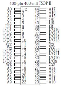 Specifications
| Parameter |
Device |
Symbol |
Min |
Max |
Unit |
| Voltage on VCC relative to VSS |
|
VtIN |
0.5 |
VCC + 0.5 |
V |
| Voltage on any I/O pin relative to GND |
|
VtI/O |
0.5 |
|
V |
| Power dissipation |
|
PD |
|
1.0 |
W |
| Storage temperature (plastic) |
|
Tstg |
65 |
+150 |
°C |
| Temperature with VCC applied |
|
Tbias |
65 |
+125 |
°C |
| DC output current (low) |
|
IOUT |
|
20 |
mA |
DescriptionThe AS6UA25617 is a low-power CMOS 4,194,304-bit Static Random Access Memory (SRAM) device organized as 262,144 words * 16 bits. It is designed for memory applications where slow data access, low power, and simple interfacing are desired.
Equal address access and cycle times (tAA, tRC, tWC) of 55/70/100 ns of AS6UA25617 are ideal for low-power applications. Active high and low chip selects (CS1 and CS2) permit easy memory expansion with multiple-bank memory systems.
When CS1 is high, or UB and LB are high or CS2 is low, the device enters standby mode: the AS6UA25617 is guaranteed not to exceed 72 mW power consumption at 3.6V and 55 ns; 41 mW at 2.7V and 70 ns; or 28 mW at 2.3V and 100 ns. The device also returns data when VCC is reduced to 1.5V for even lower power consumption.
A write cycle of AS6UA25617 is accomplished by asserting write enable (WE) and chip select (CS1) low, UB and/or LB low, and CS2 high. Data on the input pins I/O1I/O16 is written on the rising edge of WE (write cycle 1) or CS1, CS2 (write cycle 2). To avoid bus contention, external devices should drive I/O pins only after outputs have been disabled with output enable (OE) or write enable (WE).
A read cycle is accomplished by asserting output enable (OE), chip select (CS1) low, UB and/or LB low, with write enable
(WE) and CS2 high. The chip drives I/O pins with the data word referenced by the input address. When either chip select or output enable is inactive, or write enable is active, or (UB) and (LB), output drivers stay in high-impedance mode.
AS6UA25617 provides multiple center power and ground pins, and separate byte enable controls, allowing individual bytes to be written and read. LB controls the lower bits, I/O1I/O8, and UB controls the higher bits, I/O9I/O16.
All chip inputs of AS6UA25617 and outputs are CMOS-compatible, and operation is from either a single 1.65V to 3.6V supply. The device is available in the JEDEC standard 48-ball FBGA and 44-pin TSOPII packages.

 AS6UA25617 Data Sheet


