Features: · Organization: 1,048,576 words × 32 or 36 bits
· Fast clock to data access: 7.5/8.5/10 ns
· Fast OE access time: 3.5/4.0 ns
· Fully synchronous flow-through operation
· Asynchronous output enable control
· Available in 100-pin TQFP package
· Individual byte write and global write
· Multiple chip enables for easy expansion
· 2.5V core power supply
· Linear or interleaved burst control
· Snooze mode for reduced power-standby
· Common data inputs and data outputs
Pinout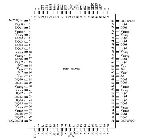 Specifications
| Parameter |
Symbol |
Min |
Max |
Unit |
| Power supply voltage relative to GND |
V DD, VDDQ
|
0.3 |
+3.6 |
V |
| Input voltage relative to GND (input pins) |
VIN |
0.3 |
VDD + 0.3
|
V |
| Input voltage relative to GND (I/O pins) |
VIN |
0.3 |
VDDQ + 0.3
|
V |
| Power dissipation |
PD |
|
1.8 |
W |
| Storage temperature (plastic) |
IOUT |
|
20 |
MV |
| Storage temperature |
Tstg |
65 |
+150 |
|
| Temperature under bias |
Tbias |
65 |
+135 |
|
DescriptionThe AS7C251MFT32A/36A is a high-performance CMOS 32-Mbit synchronous Static Random Access Memory (SRAM) device organized as 1,048,576 words × 32 or 36 bits.
Fast cycle times of 8.5/10/12 ns with clock access times (tCD ) of 7.5/8.5/10 ns. Three chip enable (CE) inputs permit easy memory expansion.Burst operation is initiated in one of two ways: the controller address strobe (ADSC), or the processor address strobe (ADSP ). The burst advance pin (ADV ) allows subsequent internally generated burst addresses.
Read cycles are initiated with ADSP (regardless of WE and ADSC) using the new external address clocked into the on-chip address register when ADSP is sampled low, the chip enables are sampled active, and the output buffer is enabled with OE In a read operation, the data accessed by the current address registered in the address registers by the positive edge of CLK are carried to the data-out buffer. ADV is ignored on the clock edge that samples ADSP asserted, but is sampled on all subsequent clock edges. Address is incremented internally for the next access of the burst when ADV is sampled low and both address strobes are high. Burst mode is selectable with the LBO input. With LBO unconnected or driven high, burst operations use an interleaved count sequence. With LBO driven low, the device uses a linear count sequence.
Write cycles are performed by disabling the output buffers with OE and asserting a write command. A global write enable GWE writes all 32/36 regardless of the state of individual BW[a:d] inputs. Alternately, when GWE is high, one or more bytes may be written by asserting BWE and the appropriate individual byte BWn signals.
BWn is ignored on the clock edge that samples ADSP low, but it is sampled on all subsequent clock edges. Output buffers are disabled when BWn is sampled LOW regardless of OE. Data is clocked into the data input register when BWn is sampled low. Address is incremented internally to the next burst address if BWn and ADV are sampled low.
Read or write cycles may also be initiated with ADSC instead of ADSP . The differences between cycles initiated with ADSC and ADSP are as follows:
· ADSP must be sampled high when ADSC is sampled low to initiate a cycle with ADSC.
·WE signals are sampled on the clock edge that samples ADSC low (and ADSP high).
· Master chip enable CE0 blocks ADSP , but not ADSC.
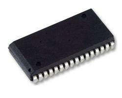
The AS7C251MFT32A and AS7C251MFT36A family operates from a core 2.5V power supply. These devices are available in 100-pin TQFP package.

 AS7C251MFT36A-10TQC Data Sheet