Features: • Organization: 131,072 words × 18 bits
• NTD™ architecture for efficient bus operation
• Fast clock speeds to 200 MHz
• Fast clock to data access: 3.0/3.5/4.0 ns
• Fast OE access time: 3.0/3.5/4.0 ns
• Fully synchronous operation
• Asynchronous output enable control
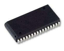
• Available in 100-pin TQFP package
• Byte write enables
• Clock enable for operation hold
• Multiple chip enables for easy expansion
• 3.3V core power supply
• 2.5V or 3.3V I/O operation with separate VDDQ
• Self-timed write cycles
• Interleaved or linear burst modes
• Snooze mode for standby operationPinout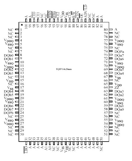 Specifications
| Parameter |
Symbol |
Min |
Max |
Unit |
| Power supply voltage relative to GND |
VDD, VDDQ |
0.5 |
+4.6 |
V |
| Input voltage relative to GND (input pins) |
VIN |
0.5 |
VDD + 0.5 |
V |
| Input voltage relative to GND (I/O pins) |
VIN |
0.5 |
VDDQ + 0.5 |
V |
| Power dissipation |
Pd |
|
1.8 |
W |
| Short circuit output current |
IOUT |
|
20 |
mA |
| Storage temperature |
Tstg |
65 |
+150 |
oC |
| Temperature under bias |
Tbias |
65 |
+135 |
oC |
DescriptionThe AS7C33128NTD18B family is a high performance CMOS 2 Mbit synchronous Static Random Access Memory (SRAM) organized as 131,072 words × 18 bits and incorporates a LATE LATE Write.
This variation of the 2Mb sychronous SRAM uses the No Turnaround Delay (NTD™) architecture, featuring an enhanced Write operation that improves bandwidth over pipeline burst devices. In a normal pipeline burst device, the write data, command, and address of AS7C33128NTD18B are all applied to AS7C33128NTD18B on the same clock edge. If a Read command follows this Write command, the system must wait for two 'dead' cycles for valid data to become available. These dead cycles of AS7C33128NTD18B can significantly reduce overall bandwidth for applications requiring random access or Read-Modify-Write operations.
NTD™ AS7C33128NTD18B devices use the memory bus more efficiently by introducing a write 'latency' which matches the two (one)cycle pipeline (flowthrough) read latency. Write data is applied two cycles after the Write command and address, allowing the Read pipeline to clear. With NTD™AS7C33128NTD18B , Write and Read operations can be used in any order without producing dead bus cycles.
Assert R/W low to perform Write cycles. Byte Write enable controls write access to specific bytes, or can be tied low for full 18 bit writes. Write enable signals, along with the write address, are registered on a rising edge of the clock. Write data of AS7C33128NTD18B is applied to the device two clock cycles later. Unlike some asynchronous SRAMs, output enable OE does not need to be toggled for write operations; it can be tied low for normal operations. Outputs go to a high impedance state when the AS7C33128NTD18B is deselected by any of the three chip enable inputs (refer to Synchronous truth table on page 6). In pipeline mode, a two cycle deselect latency allows pending read or write operations to be completed.
Use the ADV (burst advance) input to perform burst read, write and deselect operations. When ADV is high, external addresses, chip select, R/W pins are ignored, and internal address counters of AS7C33128NTD18B increment in the count sequence specified by the LBO control. Any device operations, including burst, can be stalled using the CEN=1 the clock enable input.
The AS7C33128NTD18B operates with a 3.3V ± 5% power supply for the device core (VDD). DQ circuits use a separate power supply (VDDQ) that operates across 3.3V or 2.5V ranges. AS7C33128NTD18B are available in a 100-pin 14×20 mm TQFP package.

 AS7C33128NTD18B Data Sheet