AT25F512A

Features: • Serial Peripheral Interface (SPI) Compatible• Supports SPI Modes 0 (0,0) and 3 (1,1) Datasheet Describes 0 Operation• 33 MHz Clock Rate• Byte Mode and 128-byte Page Mode for Program Operations• Sector Architecture: Two Sectors with 32K Bytes Each 256 Pages...

product image

AT25F512A Picture
SeekIC No. : 004289722 Detail

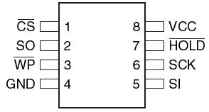
AT25F512A: Features: • Serial Peripheral Interface (SPI) Compatible• Supports SPI Modes 0 (0,0) and 3 (1,1) Datasheet Describes 0 Operation• 33 MHz Clock Rate• Byte Mode and 128-byte Pa...

floor Price/Ceiling Price

Part Number:
AT25F512A
Supply Ability:
5000

Price Break

  • Qty
  • 1~5000
  • Unit Price
  • Negotiable
  • Processing time
  • 15 Days
Total Cost: $ 0.00

SeekIC Buyer Protection PLUS - newly updated for 2013!

  • Escrow Protection.
  • Guaranteed refunds.
  • Secure payments.
  • Learn more >>

Month Sales

268 Transactions

Rating

evaluate  (4.8 stars)

Upload time: 2024/4/29

Payment Methods

All payment methods are secure and covered by SeekIC Buyer Protection PLUS.

Notice: When you place an order, your payment is made to SeekIC and not to your seller. SeekIC only pays the seller after confirming you have received your order. We will also never share your payment details with your seller.
Product Details

Description


Features:

• Serial Peripheral Interface (SPI) Compatible
• Supports SPI Modes 0 (0,0) and 3 (1,1)
Datasheet Describes 0 Operation
• 33 MHz Clock Rate
• Byte Mode and 128-byte Page Mode for Program Operations
• Sector Architecture:
Two Sectors with 32K Bytes Each
256 Pages per Sector
• Product Identification Mode
• Low-voltage Operation
2.7 (VCC = 2.7 to 3.6V)
• Sector Write Protection
• Write Protect (WP) Pin and Write Disable Instructions for both Hardware and Software Data Protection
• Self-timed Program Cycle (75 µs/byte typical)
• Self-timed Sector Erase Cycle (1 second/sector typical)
• Single Cycle Reprogramming (Erase and Program) for Status Register
• High Reliability
Endurance: 10,000 Write Cycles Typical
Data Retention: 20 Years
• 8-lead JEDEC SOIC and 8-lead SAP Packages


Pinout

  Connection Diagram


Specifications

Operating Temperature...........................−40°C to +85°C
Storage Temperature ...........................−65°C to +150°C
Voltage on Any Pin
with Respect to Ground............................... −1.0V to +5.0V
Maximum Operating Voltage ....................................... 4.2V
DC Output Current................................................... 5.0 mA


Description

The AT25F512A provides 524,288 bits of serial reprogrammable Flash memory organized as 65,536 words of 8 bits each. The device is optimized for use in many industrial and commercial applications where low-power and low-voltage operation are essential.

The AT25F512A is available in a space-saving 8-lead JEDEC SOIC and 8-lead SAP packages. The AT25F512A is enabled through the Chip Select pin (CS) and accessed via a three-wire interface consisting of Serial Data Input (SI), Serial Data Output (SO), and Serial Clock (SCK). All write cycles are completely self-timed.

Block write protection for the entire memory array is enabled by programming the status register. Separate write enable and write disable instructions are provided for additional data protection. Hardware data protection of AT25F512A is provided via the Write Protect (WP) pin to protect against inadvertent write attempts to the status register. The HOLD pin may be used to suspend any serial communication without resetting the serial sequence.


Customers Who Bought This Item Also Bought

Margin,quality,low-cost products with low minimum orders. Secure your online payments with SeekIC Buyer Protection.
Fans, Thermal Management
Power Supplies - External/Internal (Off-Board)
Isolators
Sensors, Transducers
LED Products
View more