Data Bus Width
:
Memory Type
:
Timing Type
:
Access Time
:
Supply Voltage - Max
: 3.6 V
Supply Voltage - Min
: 2.7 V
Mounting Style
: SMD/SMT
Packaging
: Tray
Interface Type
: SPI
Operating Temperature
: + 85 C
Architecture
: Sectored
Maximum Operating Current
: 15 mA
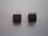
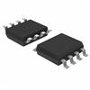
Package / Case
: VDFN-8
Memory Size
: 1056 K
DescriptionThe AT45DB161D-MU is one member of the AT45DB161D series.The AT45DB161D is a 2.5-volt or 2.7-volt, serial-interface sequential access Flash memory ideally suited for a wide variety of digital voice-, image-, program code-and data-storage applications. The AT45DB161D supports RapidS serial interface for applications requiring very high speed operations. RapidS serial interface is SPI compatible for frequencies up to 66 MHz. AT45DB161D-MU 17,301,504 bits of memory are organized as 4,096 pages of 512 bytes or 528 bytes each. In addition to the main memory, the AT45DB161D also contains two SRAM buffers of 512/528 bytes each.
Features of the AT45DB161D-MU are:(1)JEDEC standard manufacturer and device ID read; (2)100,000 program/erase cycles per page minimum; (3)data retention20 years; (4)industrial temperature range; (5)green (Pb/halide-free/RoHS compliant) packaging options; (6)hardware and software data protection features ; (7)sector lockdown for secure code and data storage; (8)continuous read capability through entire array; (9)page program operation.The buffers allow the receiving of data while a page in the main Memory is being reprogrammed,as well as writing a continuous data stream. EEPROM emulation (bit or byte alterability) is easily handled with a self-contained three step read-modify-write operation.
The absolute maximum ratings of the AT45DB161D-MU can be summarized as:(1)temperature under bias:-55 to 125;(2)storage temperature:65 to +150;(3)all input voltages (including NC pins) with respect to ground:-0.6V to +6.25V;(4)all output voltages with respect to ground:-0.6V to VCC + 0.6V.Stresses beyond those listed under "absolute maximum ratings"may cause permanent damage to the device.This is a stress rating only and functional operation of the device at these or any other conditions beyond those indicated in the operational sections of this specification is not implied.Exposure to absolute maximum rating conditions for extended periods may affect device reliability.For full clock cycle operation to be achieved, when the DataFlash is clocking data out on the falling edge of SCK, the host controller should wait until the next falling edge of SCK to latch the data in. Similarly, the host controller should clock AT45DB161D-MU data out on the rising edge of SCK in order to give the DataFlash a full clock cycle to latch the incoming data in on the next rising edge of SCK.
Parameters: | Technical/Catalog Information | AT45DB161D-MU |
| Vendor | Atmel |
| Category | Integrated Circuits (ICs) |
| Memory Type | DataFLASH |
| Memory Size | 16M (4096 pages x 528 bytes) |
| Speed | 66MHz |
| Interface | SPI, 3-Wire Serial |
| Package / Case | 8-VDFN |
| Packaging | Tray |
| Voltage - Supply | 2.7 V ~ 3.6 V |
| Operating Temperature | -40°C ~ 85°C |
| Format - Memory | FLASH |
| Drawing Number | * |
| Lead Free Status | Lead Free |
| RoHS Status | RoHS Compliant |
| Other Names | AT45DB161D MU
AT45DB161DMU
|
 AT45DB161D-MU Data Sheet