Features: ` Low Voltage Operation - 2.7V Read - 5V Program/Erase ` Fast Read Access Time - 120 ns ` Internal Erase/Program Control ` Sector Architecture - One 8K Words (16K bytes) Boot Block with Programming Lockout - Two 8K Words (16K bytes) Parameter Blocks - One 232K Words (464K bytes) Main Mem...
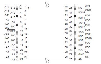
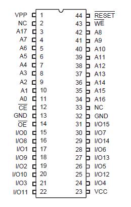
AT49BV4096: Features: ` Low Voltage Operation - 2.7V Read - 5V Program/Erase ` Fast Read Access Time - 120 ns ` Internal Erase/Program Control ` Sector Architecture - One 8K Words (16K bytes) Boot Block with Pr...
SeekIC Buyer Protection PLUS - newly updated for 2013!
268 Transactions
All payment methods are secure and covered by SeekIC Buyer Protection PLUS.


The AT49BV4096 and AT49LV4096 are 3-volt, 4-megabit Flash Memories organized as 256K words of 16 bits each. Manufactured with Atmel's advanced nonvolatile CMOS technology, the devices offer access times to 120 ns with power dissipation of just 67 mW at 2.7V read. When deselected, the CMOS standby current is less than 50 A.
To allow for simple in-system reprogrammability, the AT49BV4096/LV4096 does not require high input voltages for programming. Reading data out of the device is similar to reading from an EPROM; it has standard CE, OE, and WE inputs to avoid bus contention. Reprogramming the AT49BV4096/LV4096 is performed by first erasing a block of data and then programming on a word-by-word basis.
AT49BV4096 is erased by executing the erase command sequence; the device internally controls the erase operation. The memory is divided into three blocks for erase operations. There are two 8K word parameter block sections and one sector consisting of the boot block and the main memory array block. The AT49BV4096/LV4096 is programmed on a word-by-word basis.
AT49BV4096 has the capability to protect the data in the boot block; this feature is enabled by a command sequence. Once the boot block programming lockout feature is enabled, the data in the boot block cannot be changed when input levels of 3.6 volts or less are used. The typical number of program and erase cycles is in excess of 10,000 cycles.
The optional 8K word boot block section includes a reprogramming lock out feature to provide data integrity. The boot sector is designed to contain user secure code, and when the feature is enabled, the boot sector is protected from being reprogrammed.
During a chip erase, sector erase, or word programming, the VPP pin must be at 5V ± 10%.