Features: • Low Pin Count (LPC) BIOS Device
• Functions as Firmware Hub for Intel 810, 810E, 820, 840 Chipsets
• 8M or 4M Bits of Flash Memory for Platform Code/Data Storage
Uniform, 64-Kbyte Memory Sectors
Available in 8M Bits (AT49LW080) and 4M Bits (AT49LW040)
Automated Byte-program and Sector-erase Operations
• Two Configurable Interfaces
Firmware Hub (FWH) Interface for In-System Operation
Address/Address Multiplexed (A/A Mux) Interface for Programming during Manufacturing
• Firmware Hub Hardware Interface Mode
5-signal Communication Interface Supporting x8 Reads and Writes
Read and Write Protection for Each Sector Using Software-controlled Registers
Two Hardware Write-protect Pins: One for the Top Boot Sector, One for All Other Sectors
Five General-purpose Inputs, GPIs, for Platform Design Flexibility
Operates with 33 MHz PCI Clock and 3.3V I/O
• Address/Address Multiplexed (A/A Mux) Interface
11-pin Multiplexed Address and 8-pin Data Interface
Supports Fast On-board or Out-of-system Programming
• Power Supply Specifications
VCC: 3.3V ± 0.3V
VPP: 3.3V and 12V for Fast Programming
• Industry-standard Packages
(40-lead TSOP or 32-lead PLCC)Pinout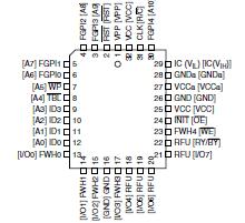 Specifications
Voltage on Any Pin
(except VPP) .................................-0.5V to +VCC + 0.5V(1)(2)(4)
VPP Voltage ..........................................-0.5V to +13.0V(1)(2)(3)
Notes: 1. All specified voltages are with respect to GND. Minimum DC voltage on the VPP pin is -0.5V. During transitions, this level may undershoot to -2.0V for periods of <20 ns. During transitions, this level may overshoot to VCC + 2.0V for periods <20 ns.
2. Maximum DC voltage on VPP may overshoot to +13.0V for periods <20 ns.
3. Connection to supply of VHH is allowed for a maximum cumulative period of 80 hours.
4. Do not violate processor or chipset limitations on the INIT pin.
*NOTICE: Stresses beyond those listed under "Absolute Maximum Ratings" may cause permanent damage to the device. This is a stress rating only and functional operation of the device at these or any other conditions beyond those indicated in the operational sections of this specification is not implied. Exposure to absolute maximum rating conditions for extended periods may affect device reliability.
DescriptionThe AT49LW080 and the AT49LW040 are Flash memory devices designed to be compatible with the Intel 82802AC and the Intel 82802AB Firmware Hub (FWH) devices for PC-Bios Application. A feature of the AT49LW080/040 is the nonvolatile memory core. The high-performance memory is arranged in eight (AT49LW 040) or sixteen (AT49LW080) 64-Kbyte sectors.
If the state of TBL or WP changes during a program suspend or erase suspend state,the changes to the device AT49LW040's locking status do not take place immediately. The suspended operation may be resumed to successfully complete the program or erase operation. The new lock status will take place after the program or erase operation completes.
These AT49LW040 pins function in combination with the register-based sector locking (to be explained later). These pins, when active, will write-protect the appropriate sector(s),regardless of the associated sector locking registers. (For example, when TBL is active,writing to the top sector is prevented, regardless of the state of the Write Lock bit for the top sector's locking register. In such a case, clearing the write-protect bit in the register will have no functional effect, even though the register may indicate that the sector is no longer locked. The register may still be set to read-lock the sector, if desired.)

 AT49LW040 Data Sheet