AT84AD004

Features: •Dual ADC with 8-bit Resolution•500 Msps Sampling Rate per Channel, 1 Gsps in Interlaced Mode•Single or 1:2 Demultiplexed Output•LVDS Output Format (100Ω)•500 mVpp Analog Input (Differential Only)•Differential or Single-ended 50Ω PECL/LVDS ...

product image

AT84AD004 Picture
SeekIC No. : 004290689 Detail

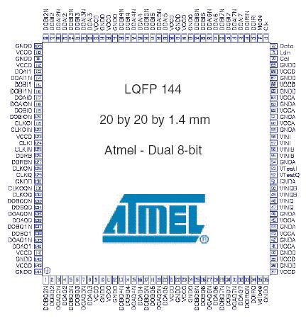
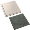
AT84AD004: Features: •Dual ADC with 8-bit Resolution•500 Msps Sampling Rate per Channel, 1 Gsps in Interlaced Mode•Single or 1:2 Demultiplexed Output•LVDS Output Format (100Ω)R...

floor Price/Ceiling Price

Part Number:
AT84AD004
Supply Ability:
5000

Price Break

  • Qty
  • 1~5000
  • Unit Price
  • Negotiable
  • Processing time
  • 15 Days
Total Cost: $ 0.00

SeekIC Buyer Protection PLUS - newly updated for 2013!

  • Escrow Protection.
  • Guaranteed refunds.
  • Secure payments.
  • Learn more >>

Month Sales

268 Transactions

Rating

evaluate  (4.8 stars)

Upload time: 2024/4/30

Payment Methods

All payment methods are secure and covered by SeekIC Buyer Protection PLUS.

Notice: When you place an order, your payment is made to SeekIC and not to your seller. SeekIC only pays the seller after confirming you have received your order. We will also never share your payment details with your seller.
Product Details

Description


Features:

•Dual ADC with 8-bit Resolution
•500 Msps Sampling Rate per Channel, 1 Gsps in Interlaced Mode
•Single or 1:2 Demultiplexed Output
•LVDS Output Format (100Ω)
•500 mVpp Analog Input (Differential Only)
•Differential or Single-ended 50Ω PECL/LVDS Compatible Clock Inputs
•Power Supply: 3.3V (Analog), 3.3V (Digital), 2.25V (Output)
•LQFP144 Package
•Temperature Range:
0°C < TA < 70°C (Commercial Grade)
-40°C < TA < 85°C (Industrial Grade)
•3-wire Serial Interface
16-bit Data, 3-bit Address
1:2 or 1:1 Output Demultiplexer Ratio Selection
Full or Partial Standby Mode
Analog Gain (±1.5 dB) Digital Control
Input Clock Selection
Analog Input Switch Selection
Binary or Gray Logical Outputs
Synchronous Data Ready Reset
Data Ready Delay Adjustable on Both Channels
Interlacing Functions:Offset and Gain (Channel to Channel) CalibrationDigital Fine SDA (Fine Sampling Delay Adjust) on One ChannelInternal Static or Dynamic Built-In Test (BIT)


Application

• Instrumentation
• Satellite Receivers
• Direct RF Down Conversion
• WLAN


Pinout

  Connection Diagram


Specifications

Parameter
Symbol
Value
Unit
Analog positive supply voltage
VCCA
3.6
V
Digital positive supply voltage
VCCD
3.6
V
Output supply voltage
VCCO
3.6
V
Maximum difference between VCCA and VCCD
VCCA to VCCD
±0.8
V
Minimum VCCO
VCCO
1.6
V
Analog input voltage
VINI or VINIB
VINQ or VINQB
1/-1
V
Digital input voltage
VD
-0.3 to VCCD + 0.3
V
Clock input voltage
VCLK or VCLKB
-0.3 to VCCD + 0.3
V
Maximum difference between
VCLK and VCLKBVCLK - VCLKB
-2 to 2
V
Maximum junction temperature
TJ
125
°C
Storage temperature
Tstg
-65 to 150
°C
Lead temperature (soldering 10s)
Tleads
300
°C


Description

The AT84AD004 is a monolithic dual 8-bit analog-to-digital converter, offering low 1.4W power consumption and excellent digitizing accuracy. It integrates dual on-chip track/holds that provide an enhanced dynamic performance with a sampling rate of up to 500 Msps and an input frequency bandwidth of 1 GHz. The dual concept, the integ-rated demultiplexer and the easy interleaving mode make this device AT84AD004 user-friendly for all dual channel applications, such as direct RF conversion or data acquisition. The smart func-tion of the 3-wire serial interface eliminates the need for external components, which are usually necessary for gain and offset tuning and setting of other para-meters, leading to space and power reduction as well as system flexibility.


Customers Who Bought This Item Also Bought

Margin,quality,low-cost products with low minimum orders. Secure your online payments with SeekIC Buyer Protection.
Line Protection, Backups
Cables, Wires - Management
LED Products
Cable Assemblies
Motors, Solenoids, Driver Boards/Modules
Optoelectronics
View more