AT84CS001

Features: •High-speed ADC Family Companion Chip •Selectable 1:2 or 1:4 DMUX Ratio•Power Consumption: 2.6W •LVDS Compatible Differential Data and Clock Inputs (100Ω Terminated)•LVDS Compatible Differential Data and Data Ready Outputs•Staggered or Simultaneo...

product image

AT84CS001 Picture
SeekIC No. : 004290690 Detail

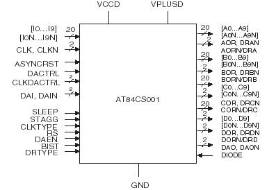
AT84CS001: Features: •High-speed ADC Family Companion Chip •Selectable 1:2 or 1:4 DMUX Ratio•Power Consumption: 2.6W •LVDS Compatible Differential Data and Clock Inputs (100Ω Term...

floor Price/Ceiling Price

Part Number:
AT84CS001
Supply Ability:
5000

Price Break

  • Qty
  • 1~5000
  • Unit Price
  • Negotiable
  • Processing time
  • 15 Days
Total Cost: $ 0.00

SeekIC Buyer Protection PLUS - newly updated for 2013!

  • Escrow Protection.
  • Guaranteed refunds.
  • Secure payments.
  • Learn more >>

Month Sales

268 Transactions

Rating

evaluate  (4.8 stars)

Upload time: 2024/4/29

Payment Methods

All payment methods are secure and covered by SeekIC Buyer Protection PLUS.

Notice: When you place an order, your payment is made to SeekIC and not to your seller. SeekIC only pays the seller after confirming you have received your order. We will also never share your payment details with your seller.
Product Details

Description


Features:

•High-speed ADC Family Companion Chip
•Selectable 1:2 or 1:4 DMUX Ratio
•Power Consumption: 2.6W
•LVDS Compatible Differential Data and Clock Inputs (100Ω Terminated)
•LVDS Compatible Differential Data and Data Ready Outputs
•Staggered or Simultaneous Data Outputs11th Bit = Ports A, B, C and D Clock in Staggered Mode
•Selectable Active Edge for Input and Output Clocks:
Only Rising: CLK and DR Mode
Rising and Falling: CLK/2 and DR/2 Mode
•Fine Tuning of Input Clock Path Delay
Compensation of External Data and Clock Path Misalignment and Skews
Once Tuned, Setting is Valid over Full Operating Frequency and Over Full Specified Temperature Range
•Additional 11th Bit (Example: for Out-of-range Bit)
•Built-in Self Test (BIST)
•Stand-alone Tunable Delay Cell
•Power Supplies: VCCD = 3.3V (Digital), VPLUSD = 2.5V (Outputs)
•Power Consumption Reduction Mode: 1.1W
•EBGA240 Package


Pinout

  Connection Diagram


Description

The AT84CS001 is a monolithic high-speed demultiplexer, used to lower a 10-bit data stream of up to 2.2 Gsps guaranteed rate by a selectable 4 or 2 ratio (a 1:8 ratio may be achieved by interleaving two DMUXes).

The DMUX is a companion chip designed to fit perfectly with all of Atmel's high-speed ADCs and is capable of tracking the ADC's output sampling rate over all operating fre-quency and temperature ranges.Thanks to AT84CS001's LVDS buffers, this DMUX can easily be interfaced with standard high-speed FPGAs (100Ω differentially terminated).

The AT84CS001 has the same footprint as Atmel's TS81102G0 DMUX, with a very similar pinout. Minimum re-design efforts are required to use this low-power DMUX. An application note "Replacing Atmel's TS81102G0 DMUX with Atmel's AT84CS001 LVDS DMUX" reference 5413, is available to assist in migrating from the TS81102G0 to the AT84CS001.

The AT84CS001 is a monolithic high-speed demultiplexer (DMUX) using high-speed Atmel technology.

It enables the user to lower a 10-bit stream of 2.2 Gsps maximum by a factor of two or four. One can obtain a 1:8 ratio by using two interleaved AT84CS001 devices. The max-imum input data rate is 2.2 Gsps in both 1:2 and 1:4 ratios.

The AT84CS001 DMUX is capable of processing an 11-bit data flow. The additional 11th bit (IOR/IORN) may be connected for example to the out-of-range bit of a 10-bit ADC.

The AT84CS001 input and output clocks as well as the input and output data are LVDS-compatible. Digital inputs are 100Ω differentially terminated on chip. Digital output buffers shall be terminated by a 100Ω differential ASIC load.The improved architecture of the DMUX facilitates interfacing with high-speed ADCs operating at up to 2.2 Gsps. No tuning of the delay between the data and clock paths should be necessary since the data and clock paths are internally matched over the fre-quency and specified temperature range.

However, in the case of misalignment or skews between the external clock path and the data path, a fine delay tuning cell has been provided by AT84CS001. Tuning may be requested for rates exceeding 2 GHz, where the data skews are more sensitive. This tunable delay cell is integrated in serial with the clock input. The delay is controlled by means of the CLK-DACTRL analog control input. The tunable delay ranges from -250 ps to 250 ps for CLKDACTRL varying from VCCD/3 to (2 * VCCD)/3.

Two modes of AT84CS001 can be selected for the clock input (CLK and CLK/2) and the clock output (DR and DR/2):
•CLK and DR mode: only the rising edges of the input (CLK,CLKN) and output (DR, DRN) clocks are active. The input (or output) clock rate remains the same as the input or output data rate.
•CLK/2 and DR/2 mode: both the rising and falling edges of the input (CLK,CLKN) and output (DR, DRN) clocks are active. The input (or output) clock rate is half the input or output data rate.

The data outputs can be received at the DMUX output in two different modes of AT84CS001:
•Staggered: even and odd bits are output with half a data period delay
•Simultaneous: even and odd bits are output at the same time

The AT84CS001 DMUX is started by the ASYNCRST control input that acts as a master asynchronous reset for the device. Once resetted, there is no loss of synchronization over an indefinite time period, therefore no additional incoming synchronous reset signal is required.

The power consumption of the AT84CS001 is 2.6W and can be reduced by approxi-mately 60% of its nominal value by means of the SLEEP control input.

A standalone delay cell is provided by AT84CS001. It features a typical 500 ps tuning range (± 250 ps around the center value of DACTRL analog control input).

A Built-in Self Test (BIST) is implemented for rapid debugging of the DMUX.Die junction temperature monitoring is possible by sensing the voltage drop across a diode implemented close to the die's hot point after forcing a 1 mA bias current.The AT84CS001 DMUX is a companion chip designed to fit perfectly with all of Atmel's high-speed ADCs.


Customers Who Bought This Item Also Bought

Margin,quality,low-cost products with low minimum orders. Secure your online payments with SeekIC Buyer Protection.
Industrial Controls, Meters
Crystals and Oscillators
Optoelectronics
Inductors, Coils, Chokes
Optical Inspection Equipment
View more