Maximum Operating Temperature
: + 85 C
Mounting Style
: SMD/SMT
Package / Case
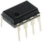
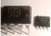
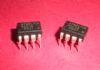
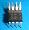
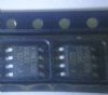
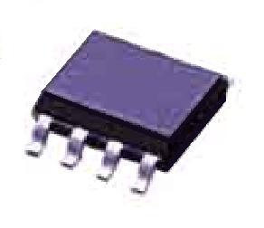
: SOIC-8
Data Retention
: 100 Years
Maximum Operating Current
: 2 mA
Operating Supply Voltage
: 2.5 V, 3.3 V, 5 V
Maximum Clock Frequency
: 2 MHz
Memory Size
: 1 Kbit
Organization
: 128 x 8, 64 x 16
Pinout Description
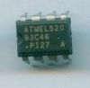
The AT93C46DN-SH-T is one member of the AT93C46D series.It has the following features including (1)three-wire serial interface;(2)die sales: wafer form, tape and reel, and bumped wafers;(3)self-timed write cycle (5 ms max);(4)low-voltage and standard-voltage operation is 1.8 (VCC = 1.8V to 5.5V).
The AT93C46DN-SH-T provides 1024 bits of serial electrically erasable programmable readonly memory (EEPROM), organized as 64 words of 16 bits each (when the ORG pin is connected to VCC), and 128 words of 8 bits each (when the ORG pin is tied to ground). The device is optimized for use in many industrial and commercial applications where low-power and low-voltage operations are essential. The AT93C46DN-SH-T is available in space-saving 8-lead PDIP, 8-lead JEDEC SOIC, 8-lead Ultra Thin mini-MAP (MLP 2x3), 8-lead TSSOP, and 8-lead dBGA2 packages.The AT93C46D is enabled through the Chip Select pin (CS) and accessed via a three-wire serial interface consisting of Data Input (DI), Data Output (DO), and Shift Clock (SK). Upon receiving a Read instruction at DI, the address is decoded and the data is clocked out serially on the DO pin. The Write cycle is completely self-timed, and no separate Erase cycle is required before Write. The Write cycle is only enabled when the part is in the Erase/Write Enable state. When CS is brought high following the initiation of a Write cycle, the DO pin outputs the Ready/Busy status of the part.
Stresses beyond those listed under "Absolute Maximum Ratings" may cause permanent damage to the device. This is a stress rating only, and functional operation of the device AT93C46DN-SH-T at these or any other conditions beyond those indicated in the operational sections of this specification is not implied. Exposure to absolute maximum rating conditions for extended periods may affect device reliability.The AT93C46DN-SH-T is accessed via a simple and versatile three-wire serial communication interface.Device operation is controlled by seven instructions issued by the host processor. A valid instruction starts with a rising edge of CS and consists of a start bit (logic "1") followed by the appropriate op code and the desired memory address location.
Parameters: | Technical/Catalog Information | AT93C46DN-SH-T |
| Vendor | Atmel |
| Category | Integrated Circuits (ICs) |
| Memory Type | EEPROM |
| Memory Size | 1K (128 x 8 or 64 x 16) |
| Speed | 250kHz, 1MHz, 2MHz |
| Interface | 3-Wire Serial |
| Package / Case | 8-SOIC |
| Packaging | Tape & Reel (TR) |
| Voltage - Supply | 1.8 V ~ 5.5 V |
| Operating Temperature | -40°C ~ 85°C |
| Format - Memory | EEPROMs - Serial |
| Lead Free Status | Lead Free |
| RoHS Status | RoHS Compliant |
| Other Names | AT93C46DN SH T
AT93C46DNSHT
|
 AT93C46DN-SH-T Data Sheet