AZ100LVE310

Features: • Operating Range of 3.0V to 5.5V• Low Skew• Guaranteed Skew Spec• Differential Design• VBB Output• 75kΩ Internal Input Pulldown Resistors• Direct Replacement for ON Semiconductor MC100LVE310 & MC100E310PinoutSpecifications Symbol ...

product image

AZ100LVE310 Picture
SeekIC No. : 004293166 Detail

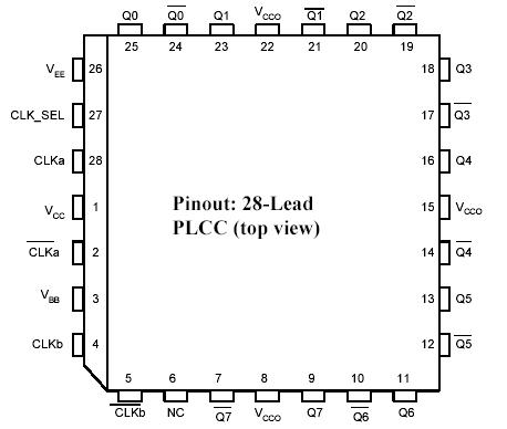
AZ100LVE310: Features: • Operating Range of 3.0V to 5.5V• Low Skew• Guaranteed Skew Spec• Differential Design• VBB Output• 75kΩ Internal Input Pulldown Resistors• ...

floor Price/Ceiling Price

Part Number:
AZ100LVE310
Supply Ability:
5000

Price Break

  • Qty
  • 1~5000
  • Unit Price
  • Negotiable
  • Processing time
  • 15 Days
Total Cost: $ 0.00

SeekIC Buyer Protection PLUS - newly updated for 2013!

  • Escrow Protection.
  • Guaranteed refunds.
  • Secure payments.
  • Learn more >>

Month Sales

268 Transactions

Rating

evaluate  (4.8 stars)

Upload time: 2024/4/28

Payment Methods

All payment methods are secure and covered by SeekIC Buyer Protection PLUS.

Notice: When you place an order, your payment is made to SeekIC and not to your seller. SeekIC only pays the seller after confirming you have received your order. We will also never share your payment details with your seller.
Product Details

Description


Features:

• Operating Range of 3.0V to 5.5V
• Low Skew
• Guaranteed Skew Spec
• Differential Design
• VBB Output
• 75kΩ Internal Input Pulldown Resistors
• Direct Replacement for ON Semiconductor MC100LVE310 & MC100E310


Pinout

  Connection Diagram


Specifications

Symbol Characteristic Rating Unit
VCC PECL Power Supply (VEE = 0V) 0 to +8.0 Vdc
VI PECL Input Voltage (VEE = 0V) 0 to +6.0 Vdc
VEE ECL Power Supply (VCC = 0V) -8.0 to 0 Vdc
VI ECL Input Voltage (VCC = 0V) -6.0 to 0 Vdc
IOUT Output Current - Continuous
- Surge
50
100
mA
TA Operating Temperature Range -40 to +85 °C
TSTG Storage Temperature Range -65 to +150 °C


Description

The AZ100LVE310 is a low skew 2:8 fanout buffer designed with clock distribution in mind. The device features fully differential clock paths to minimize both device and system skew. The AZ100LVE310 offers two selectable clock inputs allowing redundant or test clocks to be incorporated into the system clock trees.

The AZ100LVE310 provides a VBB output for single-ended use or a DC bias reference for AC coupling to the device. For singleended input applications, the VBB reference should be connected to one side of the CLKa/CLKb differential input pair. The input signal is then fed to the other CLKa/CLKb input. The VBB pin should be used only as a bias for the AZ100LVE310 as its current sink/source capability is limited. When used, the VBB pin should be bypassed to ground via a 0.01µF capacitor.

Both sides of the differential output must be terminated into 50Ω to ensure that the tight skew specification is met, even if only one side is used. In most applications all eight differential pairs will be used and therefore terminated. In the case where fewer than eight pairs are used, all output pairs on the same package side (sharing the same VCCO) as the pairs being used should be terminated to maintain minimum skew. Failure to do this will result in small degradations of propagation delay (on the order of 1020ps) of the outputs being used; while not being catastrophic to most designs this will result in an increase in skew.


Customers Who Bought This Item Also Bought

Margin,quality,low-cost products with low minimum orders. Secure your online payments with SeekIC Buyer Protection.
Line Protection, Backups
Cables, Wires
Test Equipment
Batteries, Chargers, Holders
Semiconductor Modules
View more