AZ10E116

Features: • 500ps Maximum Propagation Delay• Dedicated VCCO Pin for Each Receiver• Operating Range of 4.2V to 5.46V• 75k Internal Input Pulldown Resistors• Direct Replacement for ON Semiconductor MC10E116 & MC100E116PinoutSpecifications Symbol Characterist...

product image

AZ10E116 Picture
SeekIC No. : 004293243 Detail

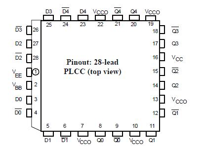
AZ10E116: Features: • 500ps Maximum Propagation Delay• Dedicated VCCO Pin for Each Receiver• Operating Range of 4.2V to 5.46V• 75k Internal Input Pulldown Resistors• Direct Repla...

floor Price/Ceiling Price

Part Number:
AZ10E116
Supply Ability:
5000

Price Break

  • Qty
  • 1~5000
  • Unit Price
  • Negotiable
  • Processing time
  • 15 Days
Total Cost: $ 0.00

SeekIC Buyer Protection PLUS - newly updated for 2013!

  • Escrow Protection.
  • Guaranteed refunds.
  • Secure payments.
  • Learn more >>

Month Sales

268 Transactions

Rating

evaluate  (4.8 stars)

Upload time: 2024/4/27

Payment Methods

All payment methods are secure and covered by SeekIC Buyer Protection PLUS.

Notice: When you place an order, your payment is made to SeekIC and not to your seller. SeekIC only pays the seller after confirming you have received your order. We will also never share your payment details with your seller.
Product Details

Description


Features:

• 500ps Maximum Propagation Delay
• Dedicated VCCO Pin for Each Receiver
• Operating Range of 4.2V to 5.46V
• 75k Internal Input Pulldown Resistors
• Direct Replacement for ON Semiconductor MC10E116 & MC100E116


Pinout

  Connection Diagram


Specifications

Symbol
Characteristic
Rating
Unit
VCC
PECL Power Supply (VEE = 0V)
0 to +6.0
Vdc
VI
PECL Input Voltage (VEE = 0V)
0 to +6.0
Vdc
VEE
ECL Power Supply (VCC = 0V)
-8.0 to 0
Vdc
VI
ECL Input Voltage (VCC = 0V)
-6.0 to 0
Vdc
IHGOUT
Output Current - Continuous
- Surge
50
100
mA
TA
Operating Temperature Range
-40 to +85
°C
TSTG
Storage Temperature Range
-65 to +150
°C


Description

The AZ10/100E116 is a quint differential line receiver with emitter-follower outputs. The E116 provides a VBB output for single-ended use or a DC bias reference for AC coupling to the device. For single-ended input applications, the VBB reference should be connected to one side of the Dn/D¯n differential input pair. The input signal is then fed to the other Dn/D¯n input. The VBB pin should be used only as a bias for the E116 as its sink/source capability is limited. When used, the VBB pin should be bypassed to ground via a 0.01F capacitor.

The receiver design features clamp circuitry to cause a defined state if both the inverting and non-inverting inputs are left open; in this case the Q output goes LOW, while the Q¯ output goes HIGH. This feature makes the evice ideal for twisted pair applications.

If both inverting and non-inverting inputs are at an equal potential of > VCC -2.5V, the receiver does not go to a defined state. This condition may produce output voltage levels between HIGH and LOW.

NOTE: Specifications in ECL/PECL tables are valid when thermal equilibrium is established.


Customers Who Bought This Item Also Bought

Margin,quality,low-cost products with low minimum orders. Secure your online payments with SeekIC Buyer Protection.
Line Protection, Backups
Test Equipment
Computers, Office - Components, Accessories
Soldering, Desoldering, Rework Products
View more