Features: ` Software features
- Program Suspend & Resume: read other sectors before programming operation is completed
- Erase Suspend & Resume: read/program other sectors before an erase operation is completed
- Data# polling & toggle bits provide status
- Unlock Bypass Program command reduces overall multiple-byte programming time
- CFI (Common Flash Interface) compliant: allows host system to identify and accommodate multiple flash devices
`Hardware features
- Sector Group Protection: hardware method of preventing write operations within a sector group
- Temporary Sector Unprotect: VID-level method of changing code in locked sectors
- ACC (high voltage) pin accelerates programming time for higher throughput during system productioN
- Hardware reset pin (RESET#) resets device
- Ready/Busy# pin (RY/BY#) detects program or erase cycle completionPinout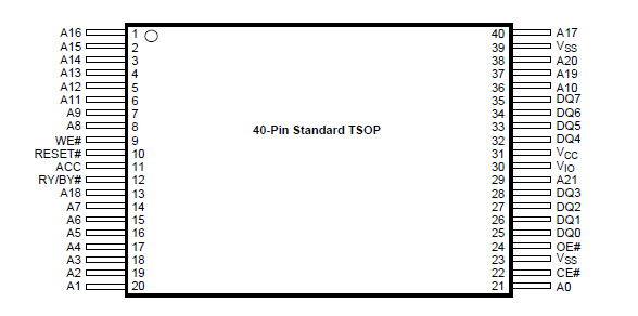 Specifications
Storage Temperature
Plastic Packages . . . . . . . . . . . . ................ . . 65 to +150
Ambient Temperature
with Power Applied . . . . . . . . . . . ................ . 65 to +125
Voltage with Respect to Ground
VCC (Note 1) . . . . . . . . . . . . . . .................... . .0.5 V to +4.0 V
VIO . . . . . . . . . . . . . . . . . . . . . . . .................. .0.5 V to +4.0 V
A9, OE#, ACC, and RESET# (Note 2) . . . . . . .0.5 V to +12.5 V
All other pins (Note 1) . . . . ................... . 0.5 V to VCC +0.5 V
Output Short Circuit Current (Note 3) . . ................. . . . 200 mA
Notes:
1. Minimum DC voltage on input or I/O pins is 0.5 V. During voltage transitions, input or I/O pins may overshoot
VSS to 2.0 V for periods of up to 20 ns. Maximum DC voltage on input or I/O pins is VCC +0.5 V. See Figure
10. During voltage transitions, input or I/O pins may overshoot to VCC +2.0 V for periods up to 20 ns. See
Figure 11.
2. Minimum DC input voltage on pins A9, OE#, ACC, and RESET# is 0.5 V. During voltage transitions, A9, OE#,
ACC, and RESET# may overshoot VSS to 2.0 V for periods of up to 20 ns. See Figure 10. Maximum DC
input voltage on pin A9, OE#, ACC, and RESET# is +12.5 V which may overshoot to +14.0 V for periods up to 20 ns.
3. No more than one output may be shorted to ground at a time. Duration of the short circuit should not be greater
than one second.
Stresses above those listed under "Absolute Maximum Ratings" may cause permanent damage to the device. This is a stress rating only; functional operation of the device at these or any other conditions above those indicated in the operational sections of this data sheet is not implied. Exposure of the device to absolute maximum rating conditions for extended periods may affect device reliability.
DescriptionThe Am29LV033MU is a 32 Mbit, 3.0 volt single power supply flash memory devices organized as 4,194,304 bytes. The device has an 8-bit wide data bus, and can be programmed either in the host system or in standard EPROM programmers.
Am29LV033MU is available with an access time of 90, 100, 110, or 120 ns. Note that each device has a specific operating voltage range (VCC) and an I/O voltage range (VIO), as specified in the Product Selector Guide and the Ordering Information sections. The device is offered in a 40-pin TSOP or 48-ball FBGA package. Each device has separate chip enable (CE#), write enable (WE#) and output enable (OE#) controls.
Each device requires only a single 3.0 volt power supply for both read and write functions. In addition to a VCC input, a high-voltage accelerated program (ACC) input provides shorter programming times through increased current. This feature is intended to facilitate factory throughput during system production, but may also be used in the field if desired.
Am29LV033MU is entirely command set compatible with the JEDEC single-power-supply Flash standard. Commands are written to the device using standard microprocessor write timing. Write cycles also internally latch addresses and data needed for the programming and erase operations.
The sector erase architecture allows memory sectors to be erased and reprogrammed without affecting the data contents of other sectors. Am29LV033MU is fully erased when shipped from the factory.
Device programming and erasure are initiated through command sequences. Once a program or erase operation has begun, the host system need only poll the DQ7 (Data# Polling) or DQ6 (toggle) status bits or monitor the Ready/Busy# (RY/BY#) output to determine whether the operation is complete. To facilitate programming, an Unlock Bypass mode reduces command sequence overhead by requiring only two write cycles to program data instead of four.
The VersatileI/O™ (VIO) control allows the host system to set the voltage levels that the device generates and tolerates on the CE# control input and DQ I/Os to the same voltage level that is asserted on the VIO pin. Refer to the Ordering Information section for valid VIO options.
Hardware data protection measures include a low VCC detector that automatically inhibits write operations during power transitions. The hardware sector protection feature disables both program and erase operations in any combination of sectors of memory. This can be achieved in-system or via programming equipment.
The Erase Suspend/Erase Resume feature allows the host system to pause an erase operation in a given sector to read or program any other sector and then complete the erase operation. The Program Suspend/Program Resume feature enables the host system to pause a program operation in a given sector to read any other sector and then complete the program operation.
The hardware RESET# pin terminates any operation in progress and resets the device, after which it is then ready for a new operation. The RESET# pin may be tied to the system reset circuitry. A system reset would thus also reset the device, enabling the host system to read boot-up firmware from the Flash memory device.
Am29LV033MU reduces power consumption in the standby mode when it detects specific voltage levels on CE# and RESET#, or when addresses have been stable for a specified period of time.
The SecSi (Secured Silicon) Sector provides a 256 byte area for code or data that can be permanently protected. Once this sector is protected, no further changes within the sector can occur.
AMD MirrorBit flash technology combines years of Flash memory manufacturing experience to produce the highest levels of quality, reliability and cost effectiveness. Am29LV033MU electrically erases all bits within a sector simultaneously via hot-hole assisted erase. The data is programmed using hot electron injection.

 Am29LV033MU Data Sheet