Features: ` HIGH SPEED: tPD = 1.25ns (MAX.) at VCC = 4.5V TA=85
` ON RESISTANCE BETWEEN TWO PORT: 25 (TYP) at VCC = 5.0V TA=25
` LOW POWER DISSIPATION: ICC = 1uA(MAX.) at TA=25
` COMPATIBLE WITH TTL OUTPUTS: VIH=2V(MIN), VIL=0.8V(MAX)
` POWER DOWN PROTECTION ON INPUTS AND OUTPUTS
` OPERATING VOLTAGE RANGE: VCC(OPR) = 4V to 5.5V
` PIN AND FUNCTION COMPATIBLE WITH 74 SERIES 16861
` IMPROVED LATCH-UP IMMUNITY
` ESD PERFORMANCE:
HBM > 2000V (MIL STD 883 method 3015);
MM > 200V
Pinout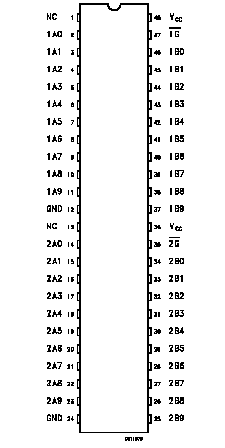 Specifications
|
Symbol |
Parameter |
Value |
Unit |
|
VCC |
Supply Voltage |
-0.5 to +7.0 |
V |
|
VI |
DC Switch and Control Pin Voltage |
-0.5 to +7.0 |
V |
|
VO |
DC Output Voltage (VCC = 0V) (note 1) |
-0.5 to +7.0 |
V |
|
VO |
DC Output Voltage (VI/O=Gnd) |
-0.5 to +7.0 |
V |
|
IIK |
DC Input Diode Current (VI/O < 0V) |
-50 |
mA |
|
IOK |
DC Output Diode Current (note 2) |
-50 |
mA |
|
IO |
DC Output Current (note 3) |
128 |
mA |
|
ICC or IGND |
DC VCC or Ground Current per Supply Pin |
±100 |
mA |
|
Tstg |
Storage Temperature |
-65 to +150 |
|
|
TL |
Lead Temperature (10 sec) |
300 |
|
Absolute Maximum Ratings are those values beyond which damage to the device may occur. Functional
operation under these conditions is not implied
1) I
O absolute maximum rating must be observed
2) V
O < GND, VO > V
CC
3) Not more than one output should be tested at one time. Duration of the test should not exceed one second.
DescriptionThe B5S162861 is an advanced high-speed CMOS 20-BIT TWO PORT BUS SWITCH fabricated with sub-micron silicon gate and double-layer metal wiring C2MOS tecnology.
It is ideal for 4V to 5.5V VCC operations and ultra-low power and low noise applications, typically notebook and docking station.
Any nG output control governs two 10-bit BUS SWITCHES. Output Enable inputs (nG) tied together gives full 20-bit operations. When nG is LOW, the switches are on. When nG is HIGH, the switches are in high impedance state.
It has ultra high-speed performance at 5V near zero delay with low ON resistance and include 25W series resistor to reduce noise resulting from reflections, thus eliminating the need for an external terminating resistor.
All inputs and outputs are equipped with protection circuits against static discharge, giving them 2KV ESD immunity and transient excess voltage.

 B5S162861 Data Sheet