On Time (Max)
:
Off Time (Max)
:
Operating Supply Voltage
:
Supply Current (Max)
:
Number of Outputs
:
Mounting Style
: SMD/SMT
Maximum Operating Temperature
: + 150 C
Package / Case
: DSO-14
On Resistance (Max)
: 0.045 Ohms
Features: • Very low standby current
• 3.3 V and 5 V compatible logic pins
• Improved electromagnetic compatibility (EMC)
• Stable behavior at under voltage
• Logic ground independent from load ground
• Secure load turn-off while logic ground disconnected
• Optimized inverse current capabilityApplication• C compatible high-side power switch with diagnostic feedback for 12 V grounded loads
• All types of resistive, inductive and capacitive loads
• Suitable for loads with high inrush currents, so as lamps
• Suitable for loads with low currents, so as LEDs
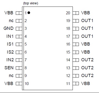
• Replaces electromechanical relays, fuses and discrete circuitsPinout
 SpecificationsStresses above the ones listed here may affect device reliability or may cause permanent damage to the device.
Unless otherwise specified:
T = 25
| Pos. |
Parameter |
Symbol |
Limit Values |
Unit |
Test Conditions |
| min. |
max. |
| Supply Voltage |
| 3.1.1 |
Supply voltage |
Vbb |
-16 |
28 |
V |
|
| 3.1.2 |
Supply voltage for full short circuit protection (single supse) (Tj(0)=-40..150) |
Vbb(SC) |
0 |
28 |
V |
L=8H,R=0.21) |
| 3.1.3 |
Voltage at power transistor |
VDS |
- |
52 |
V |
|
| 3.1.4 |
Supply Voltage for Load Dump protection |
Vbb(LD) |
|
41 |
V |
RI=22)
RL=6.8 |
| Power Stages |
| 3.1.5 |
Load current |
IL |
- |
IL(LIM) |
A |
-3) |
| 3.1.6 |
Maximum energy dissipation single pulse |
EAS |
- |
0.58 |
J |
IL(O)=2A4)
Tj(0)=150 |
| 3.1.7 |
Power dissipation (DC) |
Ptot |
- |
1.7 |
W |
Ta=855)
Tj150 |
| Logic Pins |
| 3.1.8 |
Voltage at input pin |
VIN |
-5
-16 |
10 |
V |
t2min |
| 3.1.9 |
Current through input pin |
IIN |
-2.0
-8.0 |
2.0 |
mA |
t2min |
| 3.1.10 |
Voltage at sense enable pin |
VSEN |
-5
-16 |
10 |
V |
t2min |
| 3.1.11 |
Current through sense enable pin |
ISEN |
-2.0
-8.0 |
2.0 |
mA |
t2min |
| 3.1.12 |
Current through sense pin |
IIS |
-25 |
10 |
mA |
|
| Temperatures |
| 3.1.13 |
Junction Temperature |
Tj |
-40 |
150 |
|
|
| 3.1.14 |
Dynamic temperature increase while switching |
|
|
60 |
|
|
| 3.1.15 |
Storage Temperature |
Tstg |
-55 |
150 |
|
|
| ESD Susceptibility |
| 3.1.16 |
ESD susceptibility HBM
IN,SEN
IS
OUT |
VESD |
-1
-2
-4 |
1
2
4 |
kV |
according to EIA/JESD
22-A 114B |
1)Rand L describe the complete circuit impedance including line, contact and generator impedances
2)Load Dump is specified in ISO 7636, RI is the internal resistance of the Load Dump pulse generator
3)Current limitation is a protection feature. Operation in current limitation is considered as "outside" normal operating range. Protection features are not designed for continuous repetitive operation.
4)Pulse shape represents inductive switch off: IL (t) = IL (0) * (1 - t/ t ); 0 < t peak< tpeak
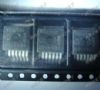
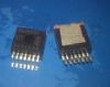
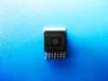
5) Device mounted on PCB (50 mm x 50 mm x 1.5mm epoxy, FR4) with 6 cm2 copper heatsinking area (one layer, 70 m thick) for Vbb connection. PCB is vertical without blown air. DescriptionThe BTS5234G is a dual channel high-side power switch in P-DSO-20-21 package proving embedded protective functions.
Features of the BTS5234G are:(1)very low standby current;(2)3.3V and 5V compatible logic pins;(3)improved electromagnetic compatibility(EMC);(4)stable behavior at under voltage;(5)logic ground independent from load ground;(6)secure load turn-off while logic ground disconnected;(7)optimized invers current capability.
The absolute maximum ratings of the BTS5234G can be summarized as:(1):the parameter is supply voltage,the symbol is Vbb,the limit values is -16 to 28,the unit is V;(2):the parameter is supply voltage for full short circuit protection (single pulse) (Tj(0)=-40 to 150),the symbol is Vbb(SC),the limit values is 0 to 28,the unit is V,the test conditions is L=8H,R=0.2;(3):the parameter is voltage at power transistor,the symbol is VDS,the limit values is 52,the unit is V;(4):the parameter is supply voltage for load dump protection,the symbol is Vbb(LD),the limit values is 0 to 41,the unit is V,the test conditions is RI=2,RL=6.8.Stresses above the ones listed here may affect device reliability or may cause permanent damage to the device.
Parameters: | Technical/Catalog Information | BTS5234G |
| Vendor | Infineon Technologies |
| Category | Integrated Circuits (ICs) |
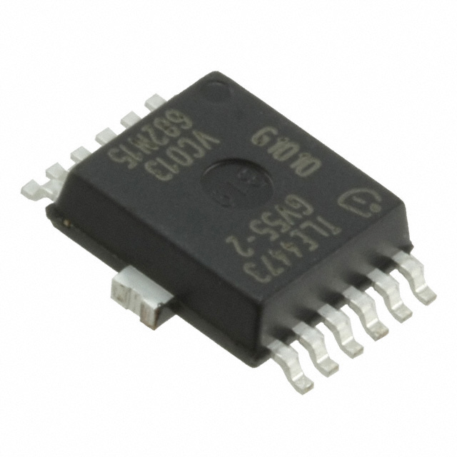
| Package / Case | DSO-20 |
| Mounting Type | Surface Mount |
| Type | High Side |
| Voltage - Supply | 4.5 V ~ 28 V |
| On-State Resistance | 45 mOhm |
| Current - Output / Channel | 3.3A |
| Current - Peak Output | 28A |
| Packaging | Tape & Reel (TR) |
| Input Type | Non-Inverting |
| Number of Outputs | 2 |
| Operating Temperature | -40°C ~ 150°C |
| Lead Free Status | Contains Lead |
| RoHS Status | RoHS Non-Compliant |
| Other Names | BTS5234G
BTS5234G
|

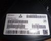
 BTS5234G Data Sheet