Type: High Side
Input Type: Non-Inverting
Number of Outputs: 2
Mounting Type: Through Hole
Packaging: Tube
Operating Temperature: -40°C ~ 150°C
Current - Output / Channel: 2.3A
On-State Resistance: 160 mOhm
Manufacturer: Infineon Technologies
Current - Peak Output: 7.5A
Voltage - Supply: 5 V ~ 34 V
Series: PROFET®
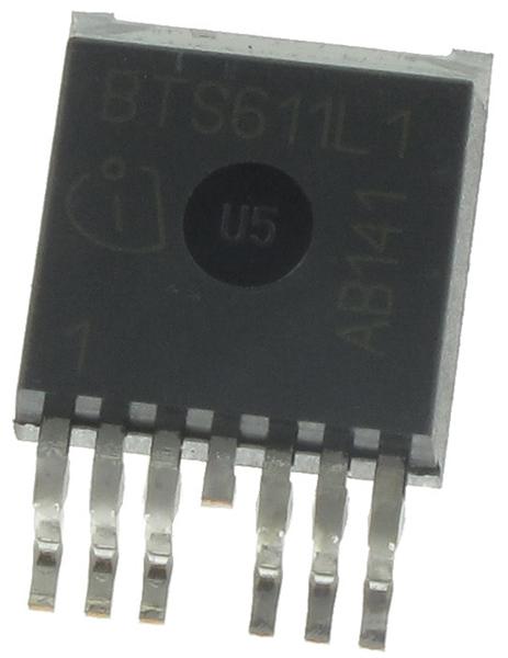
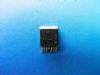
Package / Case: TO-220-7 Formed Leads
Supplier Device Package: TO-220AB/7
Features: • Overload protection
• Current limitation
• Short circuit protection
• Thermal shutdown
• Overvoltage protection (including load dump)
• Fast demagnetization of inductive loads
• Reverse battery protection1)
• Undervoltage and overvoltage shutdown with auto-restart and hysteresis
• Open drain diagnostic output
• Open load detection in ON-state
• CMOS compatible input
• Loss of ground and loss of Vbb protection
• Electrostatic discharge (ESD) protectionApplication• µC compatible power switch with diagnostic feedback for 12 V and 24 V DC grounded loads
• All types of resistive, inductive and capacitve loads
• Replaces electromechanical relays, fuses and discrete circuits
Specifications
| Parameter |
Symbol |
Values |
Unit |
| Supply voltage (overvoltage protection see page 4) |
Vbb |
43 |
V |
Supply voltage for full short circuit protection
Tj Start=-40 ...+150°C
|
Vbb |
34 |
V |
Load dump protection1) VLoadDump = VA + Vs, VA = 13.5 V
RI2)= 2 Ω, R = 5.3 Ω, t = 200 ms, IN= low or high
|
VLoaddump4) |
60 |
V |
| Load current (Current limit, see page 5) |
IL |
self-limited |
A |
Operating temperature range
Storage temperature range
|
Tj
Tstg |
-40 ...+150
-55 ...+150 |
°C |
| Power dissipation (DC), TC 25 °C |
Ptot |
36 |
W |
Inductive load switch-off energy dissipation, single pulse
Vbb = 12V, Tj,start = 150°C, TC = 150°C const.
one channel, IL = 2.3 A, ZL = 89 mH, 0 Ω:
both channels parallel, IL = 4.4 A, ZL = 47 mH, 0 Ω:
see diagrams on page 9
|
EAS
|
290
580 |
mJ |
Electrostatic discharge capability (ESD) IN:
(Human Body Model) all other pins:
acc. MIL-STD883D, method 3015.7 and ESD assn. std. S5.1-1993;
|
VESD
|
1.0
2.0
|
kV
|
Input voltage (DC)
Current through input pin (DC)
Current through status pin (DC)
see internal circuit diagrams page 7
|
IIN
IST
|
-10 ... +16
±2.0
±5.0
|
V
mA
|
DescriptionN channel vertical power FET BTS611L1 with charge pump, ground referenced CMOS compatible input and diagnostic feedback, monolithically integrated in Smart SIPMOS® technology. Fully protected by embedded protection functions.
Parameters: | Technical/Catalog Information | BTS611L1 |
| Vendor | Infineon Technologies |
| Category | Integrated Circuits (ICs) |
| Package / Case | TO-220AB-7 |
| Mounting Type | Through Hole |
| Type | High Side |
| Voltage - Supply | 5 V ~ 34 V |
| On-State Resistance | 160 mOhm |
| Current - Output / Channel | 2.3A |
| Current - Peak Output | 7.5A |
| Packaging | Tube |
| Input Type | Non-Inverting |
| Number of Outputs | 2 |
| Operating Temperature | -40°C ~ 150°C |
| Lead Free Status | Lead Free |
| RoHS Status | RoHS Compliant |
| Other Names | BTS611L1
BTS611L1
BTS611L1IN ND
BTS611L1INND
BTS611L1IN
|

 BTS611L1 Data Sheet