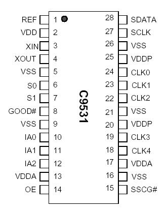
Features: • Dedicated clock buffer power pins for reduced noise, crosstalk and jitter• Input clock frequency of 25 MHz to 33 MHz• Output frequencies of XINx1, XINx2, XINx3 and XINx4• One output bank of 5 clocks.• One REF XIN clock output.• SMBus clock control in...
C9531: Features: • Dedicated clock buffer power pins for reduced noise, crosstalk and jitter• Input clock frequency of 25 MHz to 33 MHz• Output frequencies of XINx1, XINx2, XINx3 and XINx...
SeekIC Buyer Protection PLUS - newly updated for 2013!
268 Transactions
All payment methods are secure and covered by SeekIC Buyer Protection PLUS.
• Dedicated clock buffer power pins for reduced noise, crosstalk and jitter
• Input clock frequency of 25 MHz to 33 MHz
• Output frequencies of XINx1, XINx2, XINx3 and XINx4
• One output bank of 5 clocks.
• One REF XIN clock output.
• SMBus clock control interface for individual clock disabling and SSCG control
• Output clock duty cycle is 50% (± 5%)
• < 250 ps skew between output clocks within a bank
• Output jitter <175 ps
• Spread Spectrum feature for reduced electromagnetic interference (EMI)
• OE pin for entire output bank enable control and testability
• 28-pin SSOP and TSSOP packages

| Parameter | Description | Condition | Min. | Max. | Unit |
| VDD,VDDP | Core Supply Voltage | 0.5 | 4.6 | V | |
| VDDA | Analog Supply Voltage | 0.5 | 4.6 | V | |
| VIN | Input Voltage | Relative to V SS | 0.5 | VDD + 0.5 | VDC |
| TS | Temperature, Storage | Non Functional | 65 | +150 | °C |
| TA | Temperature, Operating Ambient | Functional | 0 | 70 | °C |
| TJ | Temperature, Junction | Functional | 150 | °C | |
| ESDHBM | ESD Protection (Human Body Model) | MIL-STD-883, Method 3015 | 2000 | V | |
| ØJC | Dissipation, Junction to Case | Mil-Spec 883E Method 1012.1 | °C/W | ||
| ØJA | Dissipation, Junction to Ambient | JEDEC (JESD 51) | °C/W | ||
| UL94 | Flammability Rating | At 1/8 in. | V0 | ||
| MSL | Moisture Sensitivity Level | 1 | |||