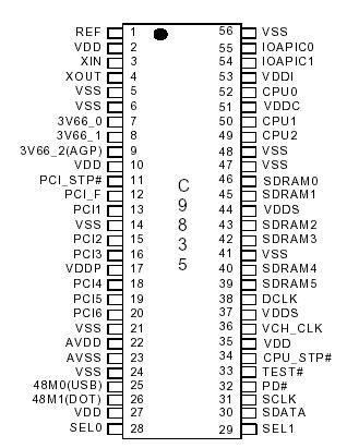
C9835

Features: • Meets Intel's®Mobile 133.3MHz Chipset• Three CPU Clocks (66.6/100/133.3 MHz, 2.5V)• Six SDRAM Clocks, 1-DCLK (100/133.3 MHz, 3.3V)• Seven PCI Clocks (33MHz, 3.3V), one free running• Two IOAPIC clocks, synchronous to CPU clock (33.3 MHz, 2.5V)• On...

product image

C9835 Picture
SeekIC No. : 004310183 Detail

C9835: Features: • Meets Intel's®Mobile 133.3MHz Chipset• Three CPU Clocks (66.6/100/133.3 MHz, 2.5V)• Six SDRAM Clocks, 1-DCLK (100/133.3 MHz, 3.3V)• Seven PCI Clocks (33MHz, 3...

floor Price/Ceiling Price

Part Number:
C9835
Supply Ability:
5000

Price Break

  • Qty
  • 1~5000
  • Unit Price
  • Negotiable
  • Processing time
  • 15 Days
Total Cost: $ 0.00

SeekIC Buyer Protection PLUS - newly updated for 2013!

  • Escrow Protection.
  • Guaranteed refunds.
  • Secure payments.
  • Learn more >>

Month Sales

268 Transactions

Rating

evaluate  (4.8 stars)

Upload time: 2024/4/26

Payment Methods

All payment methods are secure and covered by SeekIC Buyer Protection PLUS.

Notice: When you place an order, your payment is made to SeekIC and not to your seller. SeekIC only pays the seller after confirming you have received your order. We will also never share your payment details with your seller.
Product Details

Description


Features:

• Meets Intel's®Mobile 133.3MHz Chipset
• Three CPU Clocks (66.6/100/133.3 MHz, 2.5V)
• Six SDRAM Clocks, 1-DCLK (100/133.3 MHz, 3.3V)
• Seven PCI Clocks (33MHz, 3.3V), one free running
• Two IOAPIC clocks, synchronous to CPU clock (33.3 MHz, 2.5V)
• One REF Clock
• Two 48-MHz fixed non-SSCG clocks (USB and DOT)
• Three 3V66 clocks (66.6 MHz, 3.3V) ICH, HUBLINK, and AGP memory
• One selectable frequency for VCH video channel clock (48-MHz non-SSCG, 66.6-MHz CPU-SSCG, 3.3V)
• Power management using power-down, CPU stop, and PCI stop pins
• Three function select pins (include test-mode select)
• Cypress Spread Spectrum for best electromagnetic interference (EMI) reduction
• SMBUS support with readback
• 56-pin SSOP and TSSOP packages


Pinout

  Connection Diagram


Specifications

Maximum Input Voltage Relative to VSS: ............ VSS 0.3V
Maximum Input Voltage Relative to VDD:.............VDD + 0.3V
Storage Temperature: ...............................65 to + 150
Operating Temperature: ....................................0 to +85
Maximum ESD Protection................................................ 2 KV
Maximum Power Supply: ................................................5.5V

This device contains circuitry that protects the inputs against damage due to high static voltages or electric field; however, precautions should be taken to avoid application of any voltage higher than the maximum rated voltages to this circuit. For proper operation, VIN and VOUT should be constrained to the range:

VSS < (VIN or VOUT) < VDD.

Unused inputs must always be tied to an appropriate logic voltage level (either VSS or VDD).


Customers Who Bought This Item Also Bought

Margin,quality,low-cost products with low minimum orders. Secure your online payments with SeekIC Buyer Protection.
Discrete Semiconductor Products
Potentiometers, Variable Resistors
Prototyping Products
DE1
Hardware, Fasteners, Accessories
Line Protection, Backups
View more