CD4000BMS

Features: • High-Voltage Types (20V Rating)• Propagation Delay Time = 60ns (typ.) at CL = 50pF, VDD = 10V• Buffered Inputs and Outputs• Standard Symmetrical Output Characteristics• 100% Tested for Maximum Quiescent Current at 20V• 5V, 10V and 15V Parametric Rati...

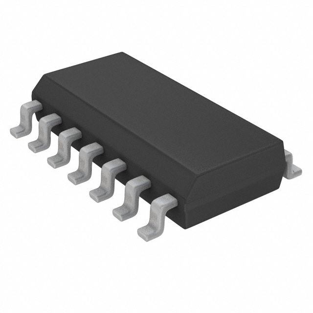
product image

CD4000BMS Picture
SeekIC No. : 004311141 Detail

CD4000BMS: Features: • High-Voltage Types (20V Rating)• Propagation Delay Time = 60ns (typ.) at CL = 50pF, VDD = 10V• Buffered Inputs and Outputs• Standard Symmetrical Output Characteri...

floor Price/Ceiling Price

Part Number:
CD4000BMS
Supply Ability:
5000

Price Break

  • Qty
  • 1~5000
  • Unit Price
  • Negotiable
  • Processing time
  • 15 Days
Total Cost: $ 0.00

SeekIC Buyer Protection PLUS - newly updated for 2013!

  • Escrow Protection.
  • Guaranteed refunds.
  • Secure payments.
  • Learn more >>

Month Sales

268 Transactions

Rating

evaluate  (4.8 stars)

Upload time: 2024/4/19

Payment Methods

All payment methods are secure and covered by SeekIC Buyer Protection PLUS.

Notice: When you place an order, your payment is made to SeekIC and not to your seller. SeekIC only pays the seller after confirming you have received your order. We will also never share your payment details with your seller.
Product Details

Description


Features:

• High-Voltage Types (20V Rating)
• Propagation Delay Time = 60ns (typ.) at CL = 50pF, VDD = 10V
• Buffered Inputs and Outputs
• Standard Symmetrical Output Characteristics
• 100% Tested for Maximum Quiescent Current at 20V
• 5V, 10V and 15V Parametric Ratings
• Maximum Input Current of 1A at 18V Over Full Package-Temperature Range; 100nA at 18V and +25
• Noise Margin (Over Full Package Temperature Range):
- 1V at VDD = 5V
- 2V at VDD = 10V
- 2.5V at VDD = 15V
• Meets All Requirements of JEDEC Tentative Standards No. 13B, "Standard Specifications for Description of "B" Series CMOS Device's


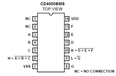
Pinout

  Connection Diagram


Specifications

DC Supply Voltage Range, (VDD) . . . . . . . .  . . . . . . . . .  . . . . .  . -0.5V to +20V
(Voltage Referenced to VSS Terminals)
Input Voltage Range, All Inputs . . . . . . . . . . . . . .  . . . . .  . .-0.5V to VDD +0.5V
DC Input Current, Any One Input . . . . . . . . . . . . .   . . . . . . . . . . . . . . . .±10mA
Operating Temperature Range. . . . . . . . . . .  . . . . .  . . . . . . . . .-55 to +125
Package Types D, F, K, H
Storage Temperature Range (TSTG) . . . . . . . . . . . . .  . . . .  .  . .-65 to +150
Lead Temperature (During Soldering) . . . . . .  . . . . .  . . . . . . . . .  . . . . . +265
At Distance 1/16 ± 1/32 Inch (1.59mm ± 0.79mm) from case for 10s Maximum


Description

CD4000BMS - Dual 3 Plus Inverter
CD4001BMS - Quad 2 Input
CD4002BMS - Dual 4 Input
CD4025BMS - Triple 3 Input
CD4000BMS, CD4001BMS, CD4002BMS, and CD4025BMS NOR gates provide the system designer with direct implementation of the NOR function and supplement the existing family of CMOS gates. All inputs and outputs are buffered.
The CD4000BMS, CD4001BMS, CD4002BMS and the CD4025BMS is supplied in these 14 lead outline packages:
  CD4000B CD4001B CD4002B CD4025B
Braze Seal DIP H4X H4Q H4Q H4Q
Frit Seal DIP H1B H1B H1B H1B
Ceramic Flatpack H3W H3W H3W H3W


Customers Who Bought This Item Also Bought

Margin,quality,low-cost products with low minimum orders. Secure your online payments with SeekIC Buyer Protection.
Potentiometers, Variable Resistors
Transformers
Motors, Solenoids, Driver Boards/Modules
Optoelectronics
Memory Cards, Modules
View more