Features: • High Voltage Type (20V Rating)
• Converts From 1 of 8 to Binary
• Provides Cascading Feature to Handle Any Number of Inputs
• Group Select Indicates One or More Priority Inputs
• Standardized Symmetrical Output Characteristics
• 100% Tested for Quiescent Current at 20V
• Maximum Input Current of 1A at 18V Over Full Package Temperature Range; 100nA at 18V and +25oC
• Noise Margin (Over Full Package/Temperature Range)
0.5V at VDD = 5V
1.5V at VDD = 10V
1.5V at VDD = 15V
• 5V, 10V and 15V Parametric Ratings
• Meets All Requirements of JEDEC Tentative Standard No. 13B, "Standard Specifications for Description of 'B' Series CMOS Devices"
Application• Priority Encoder
• Binary or BCD Encoder (Keyboard Encoding)
• Floating Point Arithmetic
Pinout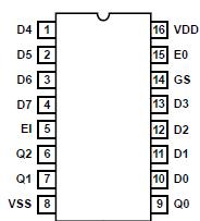 Specifications
DC Supply Voltage Range, (VDD) .........-0.5V to +20V (Voltage Referenced to VSS Terminals)
Input Voltage Range, All Inputs ................................................................0.5V to VDD +0.5V
DC Input Current, Any One Input .............................................................................. .±10mA
Operating Temperature Range. .......................... -55oC to +125oC Package Types D, F, K, H
Storage Temperature Range (TSTG) ............................................................-65oC to +150oC
Lead Temperature (During Soldering) ........................................................................+265oC
At Distance 1/16 ± 1/32 Inch (1.59mm ± 0.79mm) from case for 10s Maximum
Thermal Resistance ...................................................................................................ja ,jc
Ceramic DIP and FRIT Package...................................................................80oC/W, 20oC/W
Flatpack Package ...................................................................................... 70oC/W ,20oC/W
Maximum Package Power Dissipation (PD) at +125oC
For TA = -55oC to +100oC (Package Type D, F, K)........................................................500mW
For TA = +100oC to +125oC (Package Type D, F, K...Derate Linearity at 12mW/oC to 200mW
Device Dissipation per Output Transistor .....................................................................100mW
For TA = Full Package Temperature Range (All Package Types)
Junction Temperature ................................................................................................. +175oC
DescriptionCD4532BMS consists of combinational logic that encodes the highest priority input (D7 - D0) to a 3-bit binary code. The eight inputs, D7 through D0, each have an assigned priority; D7 is the highest priority and D0 is the lowest. The priority encoder is inhibited when the chip-enable input E1 is low. When E1 is high, the binary representation of the highestpriority input appears on output lines Q2 - Q0, and the group select line GS is high to indicate that priority inputs are present. The enable-out (EO) is high when no priority inputs are present. If any one input is high, EO is low and all cascaded lower-order stages are disabled.
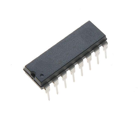
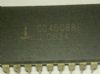
The CD4532BMS is supplied in these 16-lead outline packages:
Braze Seal DIP H4T
Frit Seal DIP H1E
Ceramic Flatpack H6W

 CD4532BMS Data Sheet