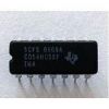
CD54ACT534F3A

DescriptionThe CD54ACT534F3A is octal D-type, three-state, positive-edge triggered flip-flops that utilize the Harris Advanced CMOS Logic technology. The eight flipflops enter data into their registers on the LOW-to-HIGH transition of the clock (CP). The Output Enable (OE) controls the three-state...

product image

CD54ACT534F3A Picture
SeekIC No. : 004311587 Detail

CD54ACT534F3A: DescriptionThe CD54ACT534F3A is octal D-type, three-state, positive-edge triggered flip-flops that utilize the Harris Advanced CMOS Logic technology. The eight flipflops enter data into their regist...

floor Price/Ceiling Price

Part Number:
CD54ACT534F3A
Supply Ability:
5000

Price Break

  • Qty
  • 1~5000
  • Unit Price
  • Negotiable
  • Processing time
  • 15 Days
Total Cost: $ 0.00

SeekIC Buyer Protection PLUS - newly updated for 2013!

  • Escrow Protection.
  • Guaranteed refunds.
  • Secure payments.
  • Learn more >>

Month Sales

268 Transactions

Rating

evaluate  (4.8 stars)

Upload time: 2024/4/30

Payment Methods

All payment methods are secure and covered by SeekIC Buyer Protection PLUS.

Notice: When you place an order, your payment is made to SeekIC and not to your seller. SeekIC only pays the seller after confirming you have received your order. We will also never share your payment details with your seller.
Product Details

Description


Description

The CD54ACT534F3A is octal D-type, three-state, positive-edge triggered flip-flops that utilize the Harris Advanced CMOS Logic technology. The eight flipflops enter data into their registers on the LOW-to-HIGH transition of the clock (CP). The Output Enable (OE) controls the three-state outputs and is independent of the register operation. When the Output Enable (OE) is HIGH, the outputs are in the high-impedance state.

The absolute maximum ratings of the CD54ACT534F3A are: (1)DC Supply Voltage, VCC: -0.5V to +6V; (2)DC Input Diode Current, IIK; (3)For VI < -0.5V or VI > VCC + 0.5V: ±20mA; (4)DC Output Diode Current, IOK; (5)For VO < -0.5V or VO > VCC + 0.5V: ±50mA; (6)DC Output Source or Sink Current, Per Output Pin, IO; (7)For VO > -0.5V or VO < VCC + 0.5V: ±50mA; (8)DC VCC or GND Current, ICC or IGND; (9)For Up to 4 Outputs Per Device, Add ±25mA For Each; (10)Additional Output: ±100mA; (11)CD54ACT534F3A Power Dissipation Per Package, PD; (12)TA = -55oC to +100oC (Package F): 500mW; (13)TA = +100oC to +125oC (Package F):  Derate Linearly at; (14)8mW/oC to 300mW; (15)Operating Temperature Range, TA; (16)Package Type F: -55oC to +125oC; (17)CD54ACT534F3A Storage Temperature, TSTG: -65oC to +150oC; (18)CD54ACT534F3A Lead Temperature (During Soldering); (19)At Distance 1/16in. ± 1/32in. (1.59mm ± 0.79mm); (20)From Case For 10s Max: +265oC; (21)Unit Inserted Into a PC Board (Min Thickness 1/16in., 1.59mm); (22)With Solder Contacting Lead Tips Only: +300oC.


Customers Who Bought This Item Also Bought

Margin,quality,low-cost products with low minimum orders. Secure your online payments with SeekIC Buyer Protection.
RF and RFID
Programmers, Development Systems
Optical Inspection Equipment
Hardware, Fasteners, Accessories
Static Control, ESD, Clean Room Products
Line Protection, Backups
View more