CD54HC107F3A

DescriptionThe CD54HC107F3A is designed as one kind of dual J-K flip-flop with set and reset negative-edge trigger that exhibits the low power consumption of standard CMOS integrated circuits, together with the ability to drive 10 LSTTL loads. Each of the flip-flop has independent J, K, Set, Reset...

product image

CD54HC107F3A Picture
SeekIC No. : 004311609 Detail

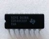
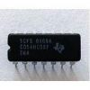
CD54HC107F3A: DescriptionThe CD54HC107F3A is designed as one kind of dual J-K flip-flop with set and reset negative-edge trigger that exhibits the low power consumption of standard CMOS integrated circuits, toget...

floor Price/Ceiling Price

Part Number:
CD54HC107F3A
Supply Ability:
5000

Price Break

  • Qty
  • 1~5000
  • Unit Price
  • Negotiable
  • Processing time
  • 15 Days
Total Cost: $ 0.00

SeekIC Buyer Protection PLUS - newly updated for 2013!

  • Escrow Protection.
  • Guaranteed refunds.
  • Secure payments.
  • Learn more >>

Month Sales

268 Transactions

Rating

evaluate  (4.8 stars)

Upload time: 2024/4/29

Payment Methods

All payment methods are secure and covered by SeekIC Buyer Protection PLUS.

Notice: When you place an order, your payment is made to SeekIC and not to your seller. SeekIC only pays the seller after confirming you have received your order. We will also never share your payment details with your seller.
Product Details

Description


Description

The CD54HC107F3A is designed as one kind of dual J-K flip-flop with set and reset negative-edge trigger that exhibits the low power consumption of standard CMOS integrated circuits, together with the ability to drive 10 LSTTL loads. Each of the flip-flop has independent J, K, Set, Reset, and Clock inputs and Q and Q outputs.

Features of the CD54HC107F3A are:(1)buffered inputs;(2)Typical fMAX = 60MHz at VCC = 5V, CL = 15pF, TA = 25 ;(3)fanout (over temperature range) standard outputs: 10 LSTTL loads and bus driver outputs: 15 LSTTL loads;(4)wide operating temperature range: -55 to +125 ;(5)balanced propagation delay and transition times;(6)significant power reduction compared to LSTTL logic ICs;(7)asynchronous reset;(8)hysteresis on clock inputs for improved noise immunity and increased input rise and fall times.

The absolute maximum ratings of the CD54HC107F3A can be summarized as:(1)DC supply voltage: -0.5V to 7V;(2)DC input diode current for VI < -0.5V or VI > VCC + 0.5V: ±20 mA;(3)DC output diode current for VO < -0.5V or VO > VCC + 0.5V: ±20 mA;(4)DC output source or sink current per output pin for VO > -0.5V or VO < VCC + 0.5V: ±25 mA;(5)DC Vcc or ground current, Icc or IGND: ±50 mA. If you want to know more information such as the electrical characteristics about the CD54HC107F3A, please download the datasheet in www.seekic.com or www.chinaicmart.com .


Customers Who Bought This Item Also Bought

Margin,quality,low-cost products with low minimum orders. Secure your online payments with SeekIC Buyer Protection.
Optoelectronics
Programmers, Development Systems
Motors, Solenoids, Driver Boards/Modules
Line Protection, Backups
Resistors
View more