CD54HC4015

Features: • Maximum Frequency, Typically 60MHz CL = 15pF, VCC = 5V, TA = 25oC• Positive-Edge Clocking• Overriding Reset• Buffered Inputs and Outputs• Fanout (Over Temperature Range) - Standard Outputs . . . . . . . . . . . . . . .. .10 LSTTL Loads - Bus Driver Outputs...

product image

CD54HC4015 Picture
SeekIC No. : 004311689 Detail

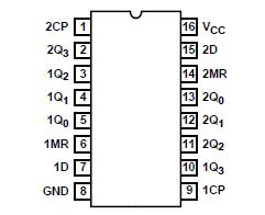
CD54HC4015: Features: • Maximum Frequency, Typically 60MHz CL = 15pF, VCC = 5V, TA = 25oC• Positive-Edge Clocking• Overriding Reset• Buffered Inputs and Outputs• Fanout (Over Tempe...
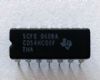
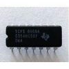
floor Price/Ceiling Price

Part Number:
CD54HC4015
Supply Ability:
5000

Price Break

  • Qty
  • 1~5000
  • Unit Price
  • Negotiable
  • Processing time
  • 15 Days
Total Cost: $ 0.00

SeekIC Buyer Protection PLUS - newly updated for 2013!

  • Escrow Protection.
  • Guaranteed refunds.
  • Secure payments.
  • Learn more >>

Month Sales

268 Transactions

Rating

evaluate  (4.8 stars)

Upload time: 2024/4/30

Payment Methods

All payment methods are secure and covered by SeekIC Buyer Protection PLUS.

Notice: When you place an order, your payment is made to SeekIC and not to your seller. SeekIC only pays the seller after confirming you have received your order. We will also never share your payment details with your seller.
Product Details

Description


Features:

• Maximum Frequency, Typically 60MHz
   CL = 15pF, VCC = 5V, TA = 25oC
• Positive-Edge Clocking
• Overriding Reset
• Buffered Inputs and Outputs
• Fanout (Over Temperature Range)
   - Standard Outputs . . . . . . . . . . . . . . . . .10 LSTTL Loads
   - Bus Driver Outputs . . . . . . . . . . . . . . . .15 LSTTL Loads
• Wide Operating Temperature Range . . . -55oC to 125oC
• Balanced Propagation Delay and Transition Times
• Significant Power Reduction Compared to LSTTL
   Logic ICs
• HC Types
   - 2V to 6V Operation
   - High Noise Immunity: NIL = 30%, NIH = 30% of VCC
   at VCC = 5V


Application

Audio
Automotive
Broadband
Digital Control
Military
Optical Networking
Security
Telephony
Video & Imaging
Wireless


Pinout

  Connection Diagram


Specifications

DC Supply Voltage, VCC . . . . . . . . . . . . . . . . . . . . . . . . . . . .-0.5V to 7V
DC Input Diode Current, IIK
   For VI< -0.5V or VI> VCC+ 0.5V. . . . . . . . . . . . . . . . . . . . .  . . . .±20mA
DC Output Diode Current, IOK
   For VO< -0.5V or VO> VCC+ 0.5V. . . . . . . . . . . . . . . . . . .  . . . . . .±20mA
DC Output Source or Sink Current per Output Pin, IO
   For VO > -0.5V or VO < VCC + 0.5V . . . . . . . . . . . . . . . . . . . . . . . ±25mA
DC VCC or Ground Current, ICC . . . . . . . . . . . . . . . . . . . . . .  . . . . ±50mA


Description

The 'HC4015 consists of two identical, independent, 4-stage serial-input/parallel-output registers. Each register has independent Clock (CP) and Reset (MR) inputs as well as a single serial Data input. "Q" outputs are available from each of the four stages on both registers. All register stages are Dtype, master-slave flip-flops. The CD54HC4015 logic level present at the Data input is transferred into the first register stage and shifted over one stage at each positive- going clock transition. Resetting of all stages is accomplished by a high level on the reset line.

CD54HC4015 can drive up to 10 low power Schottky equivalent loads. The 'HC4015 is an enhanced version of equivalent CMOS types.


Customers Who Bought This Item Also Bought

Margin,quality,low-cost products with low minimum orders. Secure your online payments with SeekIC Buyer Protection.
Computers, Office - Components, Accessories
Undefined Category
Cables, Wires
Connectors, Interconnects
View more