Features: • Common Latch-Enable Control
• Common Three-State Output Enable Control
• Buffered Inputs
• Three-State Outputs
• Bus Line Driving Capacity
• Typical Propagation Delay = 13ns at VCC = 5V, CL = 15pF, TA = 25 (Data to Output)
• Fanout (Over Temperature Range) - Standard Outputs . . . 10 LSTTL Loads - Bus Driver Outputs . . . 15 LSTTL Loads
• Wide Operating Temperature Range . . -55to 125
• Balanced Propagation Delay and Transition Times
• Significant Power Reduction Compared to LSTTL Logic ICs
• HC Types - 2V to 6V Operation - High Noise Immunity:
NIL = 30%, NIH = 30% of VCC at VCC = 5V
•HCT Types - 4.5V to 5.5V Operation - Direct LSTTL Input Logic Compatibility,
VIL= 0.8V (Max), VIH = 2V (Min) - CMOS Input Compatibility, Il 1A at VOL, VOH
ApplicationAudio
Automotive
Broadband
Digital Control
Military
Optical Networking
Security
Telephony
Video & Imaging
Wireless
Pinout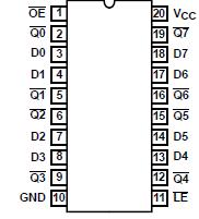 Specifications
DC Supply Voltage, VCC . . . . . . . . . . . . . . . . . . . . . . . . . . -0.5V to 7V
DC Input Diode Current, IIK
For VI < -0.5V or VI > VCC + 0.5V . . . . . . . . . . . . . . . . . . . . . .±20mA
DC Output Diode Current, IOK
For VO < -0.5V or VO > VCC + 0.5V . . . . . . . . . . . . . . . . . . . . ±20mA
DC Drain Current, per Output, IO
For -0.5V < VO < VCC + 0.5V. . . . . . . . . . . . . . . . . . . . . . . . . .±35mA
DC Output Source or Sink Current per Output Pin, IO
For VO > -0.5V or VO < VCC + 0.5V . . . . . . . . . . . . . . . . . . . . .±25mA
DC VCC or Ground Current, ICC . . . . . . . . . . . . . . . . . . . . . . . .±50mA
DescriptionThe 'HC533, 'HCT533, 'HC563, and CD74HCT563 are high-speed Octal Transparent Latches manufactured with silicon gate CMOS technology. They possess the low power consumption of standard CMOS integrated circuits, as well as the ability to drive 15 LSTTL devices.
The CD54HCT533 outputs are transparent to the inputs when the latch enable (LE) is high. When the latch enable (LE) goes low the data is latched. The output enable (OE) controls the three-state outputs. When the output enable (OE) is high the outputs are in the high impedance state. The latch operation is independent of the state of the output enable.
The 'HC533 and 'HCT533 are identical in function to the 'HC563 and CD74HCT563 but have different pinouts. The 'HC533 and 'HCT533 are similar to the 'HC373 and 'HCT373; the latter are non-inverting types.

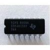
 CD54HCT533 Data Sheet