DescriptionThe CD54HCT85F3A compares two binary, BCD, or other monotonic codes and present the three possible magnitude results at the outputs. The features of CD54HCT85F3A are as follows: (1)Buffered Inputs and Outputs; (2)Typical Propagation Delay: 13ns (Data to Output at VCC = 5V, CL = 15pF, TA...
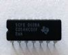
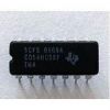
CD54HCT85F3A: DescriptionThe CD54HCT85F3A compares two binary, BCD, or other monotonic codes and present the three possible magnitude results at the outputs. The features of CD54HCT85F3A are as follows: (1)Buffer...
SeekIC Buyer Protection PLUS - newly updated for 2013!
268 Transactions
All payment methods are secure and covered by SeekIC Buyer Protection PLUS.
Features: • 'HC161, 'HCT161 4-Bit Binary Counter, Asynchronous Reset• 'HC163, 'HCT163 ...
The CD54HCT85F3A compares two binary, BCD, or other monotonic codes and present the three possible magnitude results at the outputs. The features of CD54HCT85F3A are as follows: (1)Buffered Inputs and Outputs; (2)Typical Propagation Delay: 13ns (Data to Output at VCC = 5V, CL = 15pF, TA = 25oC; (3)Serial or Parallel Expansion Without External Gating; (4)Fanout (Over Temperature Range): Standard Outputs:10 LSTTL Loads, Bus Driver Outputs: 15 LSTTL Loads; (5)Wide Operating Temperature Range: -55oC to 125oC; (6)Balanced Propagation Delay and Transition Times; (7)Significant Power Reduction Compared to LSTTL Logic ICs; (8)HC Types: 2V to 6V Operation, High Noise Immunity: NIL = 30%, NIH = 30%of VCC at VCC = 5V; (9)HCT Types: 4.5V to 5.5V Operation, Direct LSTTL Input Logic Compatibility, VIL= 0.8V (Max), VIH = 2V (Min); (10)CMOS Input Compatibility, Il 1A at VOL, VOH.
The absolute maximum ratings of the CD54HCT85F3A are: (1)DC supply voltage, VCC: -0.5V to 7V; (2)DC input diode current, IIK for VI < -0.5V or VI > VCC + 0.5V: ±20mA; (3)DC output diode current, IOK for VO < -0.5V or VO > VCC + 0.5V: ±20mA; (4)DC output source or sink current per output Pin, IO For VO > -0.5V or VO < VCC + 0.5V: ±25mA; (5)DC VCC or ground current, ICC or IGND: ±50mA.
The following is about the electrical characteristics of CD54HCT85F3A: (1)High Level Input Voltage: 1.5V min; (2)low Level Input Voltage: 0.5V max; (3)High Level Output Voltage CMOS Loads: 1.9V min at VIH or VIL, IO= -0.02mA; (4)High Level Output Voltage TTL Loads: 3.98V min at VIH or VIL, IO= -4mA; (5)Low Level Output Voltage CMOS Loads: 0.1V max at VIH or VIL, IO=0.02mA; (6)Low Level Output Voltage TTL Loads: 0.26V max at VIH or VIL, IO=0.02mA; (7)Input Leakage Current: ±0.1A max at VCC or GND; (8)Quiescent Device Current: 8A max at VCC or GND.