CDCS501

PinoutDescriptionThe CDCS501 is a spread spectrum capable, LVCMOS Input Clock Buffer for EMI reduction.The device is designed to counter common EMI problems in modern electronic designs.It accepts a 3.3V LVCMOS signal at the input and spread this signal by a small amount, centered around the input...

product image

CDCS501 Picture
SeekIC No. : 004312308 Detail

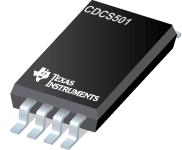
CDCS501: PinoutDescriptionThe CDCS501 is a spread spectrum capable, LVCMOS Input Clock Buffer for EMI reduction.The device is designed to counter common EMI problems in modern electronic designs.It accepts a...

floor Price/Ceiling Price

Part Number:
CDCS501
Supply Ability:
5000

Price Break

  • Qty
  • 1~5000
  • Unit Price
  • Negotiable
  • Processing time
  • 15 Days
Total Cost: $ 0.00

SeekIC Buyer Protection PLUS - newly updated for 2013!

  • Escrow Protection.
  • Guaranteed refunds.
  • Secure payments.
  • Learn more >>

Month Sales

268 Transactions

Rating

evaluate  (4.8 stars)

Upload time: 2024/5/3

Payment Methods

All payment methods are secure and covered by SeekIC Buyer Protection PLUS.

Notice: When you place an order, your payment is made to SeekIC and not to your seller. SeekIC only pays the seller after confirming you have received your order. We will also never share your payment details with your seller.
Product Details

Description


Pinout

  Connection Diagram


Description

The CDCS501 is a spread spectrum capable, LVCMOS Input Clock Buffer for EMI reduction.The device is designed to counter common EMI problems in modern electronic designs.It accepts a 3.3V LVCMOS signal at the input and spread this signal by a small amount, centered around the input frequency. The amount of spread can be selected via 3 control pins. The Functional Table contains detailed information on the amount of spread. A 4th control pin can be used to activate or deactivate the Spread Spectrum Clock Generator.

Features of the CDCS502 are:(1)Part of a Family of Easy to use Clock Generator Devices With Optional SSC; (2)SSC Capable Clock Generator / Buffer; (3)SSC Controllable via 3 External Pins ± 0% to ± 1.5% Center Spread; (4)1 External Control Pin for SSC ON / OFF Selection; (5)40 MHz to 108 MHz Single-Ended LVCMOS Input; (6)Single 3.3V Device Power Supply; (7)Wide Temperature Range 40 ° C to 85 ° C; (8)Low Space Consumption by 8 Pin TSSOP Package.

The absolute maximum ratings of the CDCS502 can be summarized as:(1)Supply voltage range 0.5 to 4.6 V; (2)Input voltage range 0.5 to 4.6 V; (3)Output voltage range 0.5 to 4.6 V; (4)Input current (V I < 0, V I > VDD) 20 mA; (5)Continuous output current 50 mA; (6)Storage temperature range 65 to 150 ° C; (7)Maximum junction temperature 125 ° C.

If you want to know more CDCS501 information such as the electrical characteristics ,please download the datasheet in www.seekdatasheet.com .


Customers Who Bought This Item Also Bought

Margin,quality,low-cost products with low minimum orders. Secure your online payments with SeekIC Buyer Protection.
Transformers
Computers, Office - Components, Accessories
Optical Inspection Equipment
Static Control, ESD, Clean Room Products
LED Products
View more